SOI Wafer (Si/SiO₂/Si) for Quartz Crystal Microbalance (QCM) Sensor Applications
No specifications available.
Overview
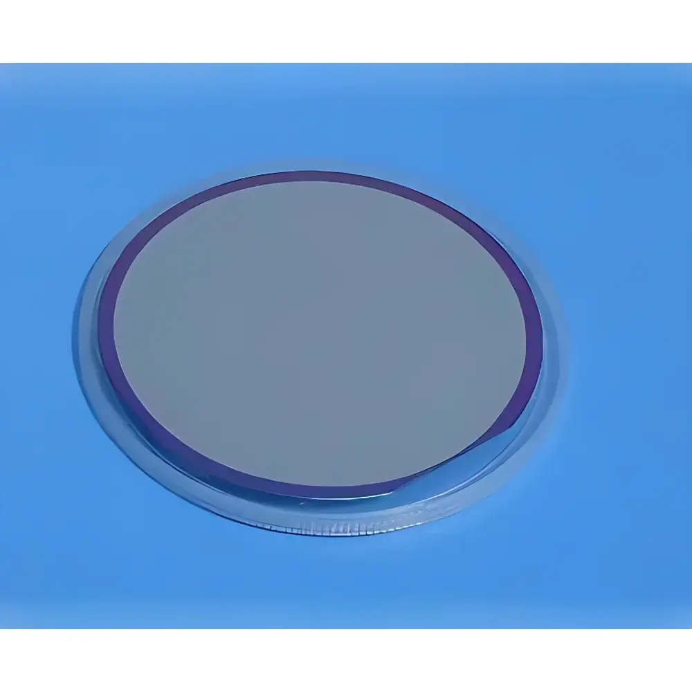
The SOI Wafer (Si/SiO₂/Si) is a high-precision silicon-on-insulator substrate engineered for integration into quartz crystal microbalance (QCM) sensor platforms, particularly in electrochemical and surface-sensitive analytical systems. Unlike conventional silicon wafers, SOI structures consist of three distinct functional layers: a device-grade top silicon layer (typically 2–3 µm), a buried oxide (BOX) layer (2 µm SiO₂), and a mechanically robust handle wafer (500 µm undoped Si). This architecture provides exceptional electrical isolation, thermal stability, and surface planarity—critical for reliable QCM frequency shift measurement under liquid-phase or gas-phase sensing conditions. The wafer’s low defect density, sub-micrometer local thickness variation (LTV < 1 µm), and tightly controlled resistivity (15–25 Ω·cm, p-type) ensure reproducible electrode deposition and minimal parasitic coupling during impedance-based or mass-loading measurements.
Key Features
- Triple-layer architecture: Top Si (2–3 µm ±0.5 µm over 5-point measurement), BOX SiO₂ (2.0 ±0.1 µm), and handle Si (500 µm undoped)
- High surface flatness: Local total thickness variation (LTV) < 1 µm across 4-inch diameter wafers
- Crystallographic orientation options: and substrates available for optimized epitaxial growth or metal adhesion
- Controlled doping profile: Boron-doped p-type top layer with resistivity 15–25 Ω·cm
- Ultra-clean packaging: Individually sealed in Class 100 cleanroom bags or 25-wafer cassette-style carriers compliant with SEMI standard packaging protocols
- Customizable specifications: Thickness tolerances, oxide stoichiometry, and surface termination (e.g., native oxide, HF-last, or thermal oxide) can be tailored to meet specific transducer design requirements
Sample Compatibility & Compliance
This SOI wafer is compatible with standard photolithography, e-beam evaporation, sputtering, and ALD processes used in QCM electrode fabrication (e.g., Au, Pt, or ITO thin-film deposition). Its thermal expansion coefficient closely matches that of fused silica and quartz resonators, minimizing interfacial stress during hybrid bonding or flip-chip assembly. The material complies with ISO 14644-1 Class 5 (Class 100) cleanroom handling standards and meets SEMI MF1530 specifications for silicon wafer geometric tolerances. While not an instrument per se, the wafer supports GLP/GMP-aligned sensor development workflows when used in validated QCM systems conforming to ASTM E2789 (Standard Guide for QCM-Based Biosensor Development) and ISO/IEC 17025 calibration traceability frameworks.
Software & Data Management
As a passive substrate material, the SOI wafer does not incorporate embedded firmware or software interfaces. However, its dimensional and electrical consistency directly impacts data fidelity in QCM systems utilizing frequency-tracking algorithms (e.g., Sauerbrey or Voigt modeling). When integrated into instruments with FDA 21 CFR Part 11-compliant software (e.g., QCM-D platforms from Biolin Scientific or KSV NIMA), the wafer’s batch-specific metrology certificates—including thickness maps, resistivity profiles, and surface roughness (Ra < 0.3 nm) reports—can be linked to electronic lab notebooks (ELNs) for full audit trail integrity. Traceable lot documentation is provided with each shipment, enabling retrospective analysis in regulated environments.
Applications
- QCM sensor development for real-time monitoring of protein adsorption, polymer film swelling, and cell adhesion kinetics
- Electrochemical QCM (EQCM) studies requiring electrically isolated working electrodes on insulating BOX layers
- Hybrid biosensors combining QCM with surface plasmon resonance (SPR) or optical waveguide detection
- Fabrication of microfluidic-integrated QCM chips with patterned top-silicon electrodes and microchannel etching
- Reference substrates for calibrating AFM-based nanomechanical characterization of ultrathin films
- Research-grade platforms for investigating interfacial water structure and ion transport at solid–liquid interfaces
FAQ
Is this SOI wafer suitable for high-frequency QCM resonators (e.g., 25 MHz or higher)?
Yes—its low LTV and uniform BOX thickness minimize acoustic mode dispersion, supporting stable operation up to 50 MHz when processed into AT-cut quartz-compatible geometries.
Can the top silicon layer be removed selectively to expose the BOX for capacitive sensing?
Yes—standard KOH or TMAH etchants provide high selectivity (>100:1) between Si and SiO₂, enabling precise recessed electrode architectures.
Do you provide wafer-level metrology data (e.g., ellipsometry, XRR, or four-point probe maps)?
Upon request, certified thickness and resistivity maps generated per SEMI MF1530 are supplied with each batch.
Are custom diameters (e.g., 6-inch) and orientations () available with lead times under 8 weeks?
Yes—standard offerings include 4″ and 6″ formats in both and orientations; non-standard BOX thicknesses (e.g., 3 µm SiO₂) are available with extended lead time.
How is surface contamination controlled during shipping?
Wafers are packaged in nitrogen-purged, static-dissipative Class 100 cleanroom bags and shipped in rigid, shock-absorbing carriers meeting ISTA 2A transport standards.