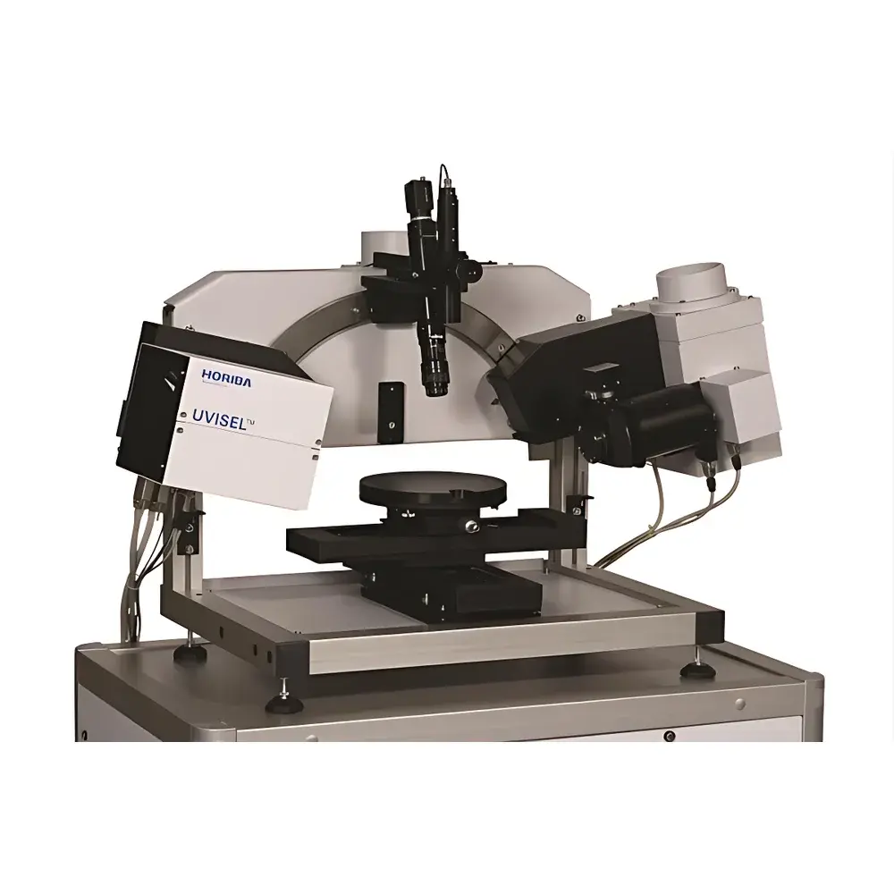
HORIBA UVISEL Plus Research-Grade Spectroscopic Ellipsometer
| Brand | HORIBA |
|---|---|
| Origin | France |
| Manufacturer Type | Original Equipment Manufacturer (OEM) |
| Origin Category | Imported Instrument |
| Model | UVISEL |
| Pricing | Available Upon Request |
Overview
The HORIBA UVISEL Plus is a research-grade spectroscopic ellipsometer engineered for high-precision, non-destructive characterization of thin films, interfaces, and surface layers. Operating on the fundamental principle of spectroscopic ellipsometry—measuring changes in the amplitude ratio (Ψ) and phase difference (Δ) of polarized light upon reflection from a sample—the UVISEL Plus delivers quantitative optical constants (n, k), layer thicknesses (from sub-Å to tens of µm), interfacial roughness, and compositional gradients across a broad spectral range. Its modular architecture supports both static and dynamic measurements under controlled environmental conditions, making it suitable for academic research, semiconductor process development, photovoltaic material screening, and advanced functional coating analysis.
Key Features
- High-frequency photoelastic modulator (PEM) operating at 50 kHz, enabling rapid, vibration-insensitive acquisition without moving elements in the optical path
- Extended spectral coverage from 190 nm to 885 nm (upgradeable to 2100 nm with optional NIR optics and detector modules)
- Configurable micro-spot sizes: 50 µm, 100 µm, or 1 mm diameter—optimized for heterogeneous samples, patterned wafers, and localized defect analysis
- Dual-detector system: UV-optimized photomultiplier tube (PMT) and visible/NIR-optimized indium gallium arsenide (InGaAs) detector (IGA), ensuring high signal-to-noise ratio across the full spectral range
- Motorized auto-goniometer with continuous angular scanning from 40° to 90° incidence, programmable step resolution down to 0.01°
- Modular sample stage options including motorized XY mapping stages, cryogenic and heating stages (–180 °C to +400 °C), electrochemical cells, liquid cells, and hermetic environmental chambers
- Millisecond-scale time-resolved acquisition mode for real-time monitoring of film growth, etching, adsorption, or phase transitions
Sample Compatibility & Compliance
The UVISEL Plus accommodates rigid and flexible substrates up to 200 mm in diameter (custom stages support larger formats). It is compatible with dielectrics, semiconductors, metals, polymers, organic-inorganic hybrids, and biological monolayers. Measurement protocols align with established international standards including ASTM E1936 (Standard Guide for Spectroscopic Ellipsometry), ISO/IEC 17025 requirements for calibration traceability, and GLP-compliant workflows when integrated with audit-trail-enabled software configurations. Optional FDA 21 CFR Part 11 compliance packages support regulated environments in pharmaceutical thin-film device development.
Software & Data Management
Controlled via HORIBA’s DeltaPsi² software platform, the UVISEL Plus provides an intuitive interface for instrument automation, optical modeling, and multi-layer fitting. The software includes built-in optical dispersion models (Cauchy, Tauc-Lorentz, Cody-Lorentz), parameter correlation analysis, uncertainty propagation tools, and batch processing for large-scale datasets. Raw spectra and fitted parameters are stored in vendor-neutral HDF5 format. DeltaPsi² supports export to CSV, XML, and industry-standard formats compatible with MATLAB, Python (via h5py), and third-party metrology databases. Audit trail logging, user access levels, and electronic signature capability are available in validated configurations.
Applications
- Atomic layer deposition (ALD) and chemical vapor deposition (CVD) process control and endpoint detection
- Optical constant determination of novel perovskite, chalcogenide, and 2D material systems
- Thickness uniformity mapping of anti-reflective, barrier, and transparent conductive oxide (TCO) coatings
- Interfacial oxidation kinetics and native oxide growth on Si, Ge, and III–V substrates
- In-situ monitoring of self-assembled monolayer (SAM) formation and protein adsorption on biosensor surfaces
- Quality assurance of OLED stack layer integrity and degradation mechanisms under bias stress
FAQ
What is the minimum detectable thickness for ultra-thin films?
Sub-angstrom sensitivity is achievable for homogeneous, smooth films on reflective substrates when using appropriate modeling constraints and high-SNR acquisition settings.
Can the UVISEL Plus measure transparent substrates such as fused silica or CaF₂?
Yes—transmission-mode ellipsometry and combined reflection/transmission modeling are supported via optional beam delivery optics and substrate characterization modules.
Is remote operation and integration with factory automation systems possible?
The instrument supports TCP/IP-based communication protocols and offers API access through DeltaPsi² SDK for integration into SECS/GEM-compliant semiconductor fabs or laboratory information management systems (LIMS).
How is calibration maintained over long-term operation?
Factory calibration is traceable to NIST standards; routine verification uses certified reference samples (e.g., Si/SiO₂ wafers), and automated wavelength and angle calibration routines are embedded in the software.
Are application-specific measurement templates available?
HORIBA provides pre-configured templates for common use cases—including solar cell absorber layers, gate dielectrics, and biomedical coatings—with validated optical models and fitting protocols.


