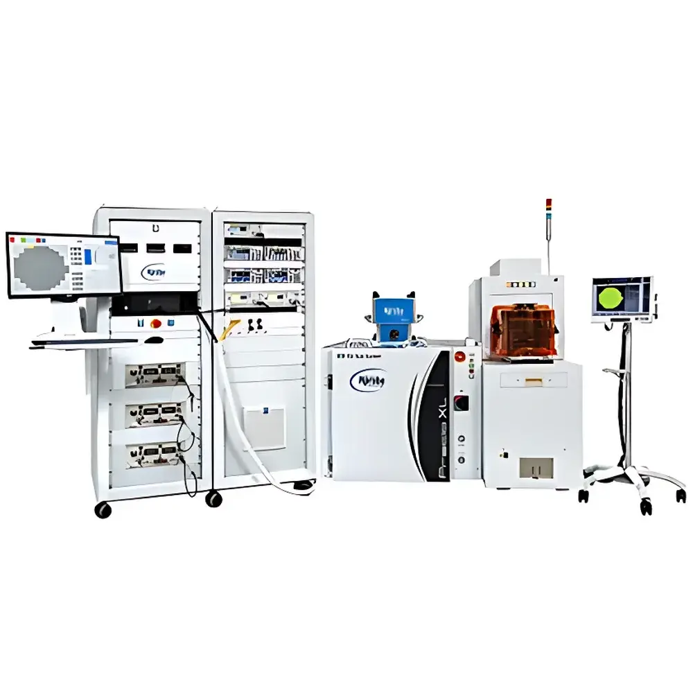
Hprobe Hprobe Magnetic Wafer-Level Test System
| Brand | Hprobe |
|---|---|
| Origin | France |
| Model | Hprobe |
| Type | Automated Magnetic Testing System for Semiconductor Wafers |
| Compatibility | 100–300 mm wafers |
| Cooling | Air-cooled |
| Power Supply | Standard AC mains |
| Field Generation | 3D vector and uniaxial (Hcoil-2T) magnetic field sources |
| Max Field Strength | ±2 T (uniaxial), up to 500 mT (3D vector) |
| Field Scan Rate | Up to 10,000 device/s |
| Field Rise Time | <20 µs (Hcoil-2T) |
| Integration | Compatible with TEL, ACCRETECH, and Electroglas probers |
| Software Platform | IBEX (MRAM), LINX (sensors), GUI-based automation with calibration, sequencing, and production control modules |
| Compliance | Designed for GLP/GMP environments |
Overview
The Hprobe Magnetic Wafer-Level Test System is an engineered solution for high-throughput, precision electrical characterization of magnetic devices under controlled, dynamically variable magnetic fields. Unlike conventional parametric testers, Hprobe integrates proprietary electromagnetic field generation directly into the probe station test head—enabling synchronized, sub-millisecond magnetic stimulation and electrical measurement at the wafer level. Its core technology relies on two patented field architectures: the 3D Vector Field Generator, which delivers independently controllable orthogonal magnetic components (Bx, By, Bz) for arbitrary field orientation and rotation; and the Hcoil-2T uniaxial generator, capable of achieving ±2 T in under 20 µs with nanosecond-level timing synchronization. This dual-field capability addresses the fundamental metrology challenge in spintronic device validation: correlating magnetic state transitions (e.g., magnetization reversal in MTJs or domain wall motion in SOT-MRAM) with electrical response—under conditions replicating real-world operating environments and manufacturing-relevant throughput constraints.
Key Features
- Patented air-cooled 3D vector and Hcoil-2T magnetic field generators—no liquid cooling infrastructure required.
- Integrated test head mounts directly onto standard 100–300 mm automated probe stations (TEL, ACCRETECH, Electroglas).
- Sub-20 µs field rise time and programmable scan rates up to 10,000 devices per second—enabling statistically robust sampling across full wafers.
- On-board 3-axis Hall sensor array with automated positioning system for traceable, in-situ field calibration at DUT location.
- Modular instrumentation architecture supporting Keysight, Tektronix, and National Instruments sources and digitizers—configured per application (DC, pulsed, RF).
- Unified software platform with hardware abstraction layer—enabling identical test sequences across R&D, qualification, and high-volume manufacturing (HVM) environments.
Sample Compatibility & Compliance
The system supports full-wafer electrical probing of MRAM bitcells (STT-, SOT-, and VC-MRAM), magnetic tunnel junctions (MTJs), and xMR-based sensors (TMR, GMR, AMR, Hall). It accommodates standard probe cards—including DC, RF, and high-density MEMS variants—and operates across process control monitor (PCM) structures and functional arrays. All magnetic field generation and measurement subsystems comply with SEMI E142 (Equipment Data Acquisition) and are architected to support GLP/GMP workflows: calibration logs, user access controls, electronic signatures, and immutable audit trails are embedded in the IBEX and LINX software suites. Field uniformity, repeatability (<0.5% RMS deviation over 50 mm diameter), and temporal synchronization are validated per internal technical specification TS-HM-001, aligned with ISO/IEC 17025 clause 5.10 on measurement uncertainty reporting.
Software & Data Management
Hprobe’s software stack comprises two domain-specific platforms—IBEX for MRAM and LINX for magnetic sensors—built on a shared, extensible framework. Both feature graphical user interfaces for manual operation, scriptable Python APIs for custom sequence development, and native integration with factory automation protocols (SECS/GEM, HSMS). Key capabilities include: automated hysteresis loop acquisition with real-time fitting (coercivity, switching field distribution, RAP/RP ratio); pulse-mode write/read stress testing with voltage/current waveform capture (down to 300 ps resolution); statistical analysis dashboards for wafer maps, yield trending, and SPC charting (X-bar/R, Cpk); and export to industry-standard formats (CSV, HDF5, STDF). All raw and processed data are stored with metadata tags (field vector, timestamp, prober coordinates, instrument configuration), ensuring full traceability from test execution to final report generation.
Applications
The system serves three primary application domains: (1) MRAM development and production—supporting wafer acceptance testing (WAT), process window qualification, and CP screening for embedded and standalone memories; (2) Magnetic sensor characterization—enabling full angular sensitivity mapping, offset drift analysis, linearity verification, and environmental robustness testing (e.g., immunity to external field interference); and (3) Fundamental spintronics research—facilitating dynamic magnetization studies, domain imaging correlation, and ultrafast switching kinetics under controlled field trajectories. It is deployed in advanced node development labs (≤28 nm BEOL), foundry process engineering groups, and fabless design houses validating IP blocks prior to tape-out.
FAQ
What distinguishes Hprobe’s field generation from conventional electromagnets or Helmholtz coils?
Conventional systems rely on low-inductance windings requiring high-current amplifiers and water cooling—limiting scan speed and field homogeneity. Hprobe’s patented coil topologies achieve high dB/dt without sacrificing spatial fidelity or thermal stability, enabling air-cooled operation and direct integration into probe station kinematics.
Can the system perform simultaneous multi-axis field sweeps and high-speed pulsing?
Yes. The hardware architecture decouples field generation from stimulus delivery: magnetic vectors are updated via FPGA-controlled current drivers, while independent pulse generators (e.g., Keysight B1500A, Tektronix AWG) deliver sub-nanosecond voltage/current transients—synchronized via PXI trigger bus with <1 ns jitter.
Is calibration traceable to national standards?
Field sensors are calibrated against NIST-traceable reference probes at Hprobe’s metrology lab in Grenoble. Each system ships with a calibration certificate covering field amplitude, linearity, and orthogonality across its operational range (±2 T uniaxial, ±500 mT 3D), with annual recalibration recommended per ISO/IEC 17025.
How does the system support transition from R&D to high-volume manufacturing?
IBEX and LINX share identical test definition syntax and data models. A sequence developed on a manual prober can be redeployed on a fully automated cluster without modification—reducing qualification overhead and ensuring measurement continuity across technology transfer gates.
Does Hprobe provide application-specific test methods?
Yes. Pre-validated test methods—including STT-MRAM toggle margin extraction, SOT-MRAM critical current density mapping, and TMR sensor angular error profiling—are included in the software suite and documented per ASTM F3096 (Standard Practice for Magnetic Device Characterization) and JEDEC JESD22-A123 (MRAM Reliability Testing).