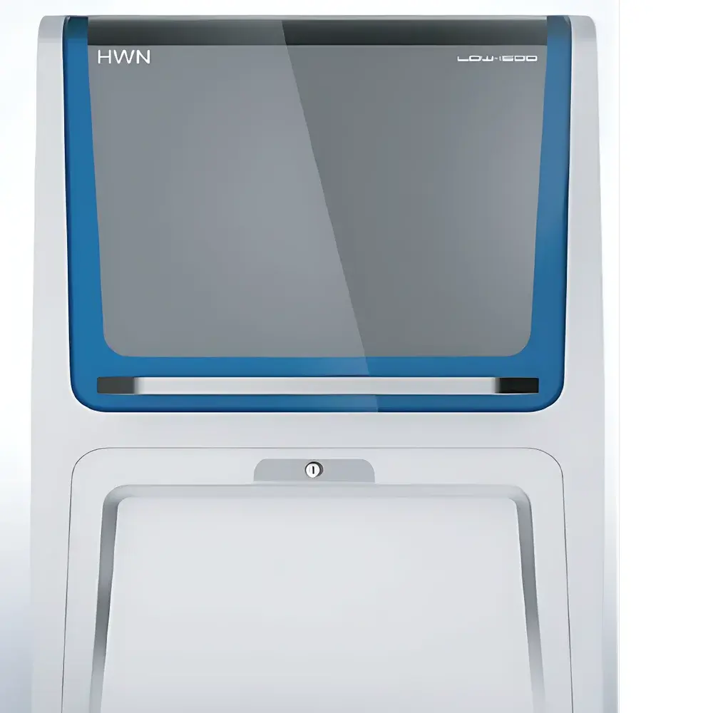
Huaweina LDW-P Nano Laser Direct-Write System
| Brand | Huaweina |
|---|---|
| Origin | Jiangsu, China |
| Manufacturer Type | Authorized Distributor |
| Product Origin | Domestic (China) |
| Model | LDW-P |
| Price Range | USD 14,000 – 28,000 |
| Maximum Writing Resolution | 50 nm |
| Minimum Spot Size | 275 nm |
| Minimum Grid Pitch | 75 nm |
| Stage Resolution | 1 nm |
| Absolute Positioning Accuracy | <10 nm |
| Writing Field Options | 100×100 to 1500×1500 µm |
| Laser Power Stability | <±1% RMS |
| Software Platform | LDW-SC Control Suite |
| Optical Principle | Nonlinear Threshold-Dependent Ablation/Modification via Gaussian-Focused Ultrafast Laser Pulses |
Overview
The Huaweina LDW-P Nano Laser Direct-Write System is a high-precision, benchtop nanofabrication platform engineered for maskless patterning of both organic and inorganic thin-film materials at sub-diffraction resolution. Unlike conventional photolithography or standard laser writing systems constrained by the Abbe diffraction limit (~λ/2NA), the LDW-P leverages nonlinear photoresponse—specifically, intensity-threshold-dependent material modification under tightly focused Gaussian laser irradiation—to achieve effective feature sizes down to 50 nm. This physical principle enables spatial confinement of energy deposition well below the nominal optical spot size (275 nm), bypassing classical resolution barriers without requiring vacuum environments, electron beams, or complex proximity masks. The system is purpose-built for research and pilot-scale development in semiconductor device prototyping, plasmonic nanostructure fabrication, diffractive optical element (DOE) synthesis, and functional metamaterial engineering. Its architecture integrates ultra-stable pulsed laser delivery, sub-nanometer motion control, and deterministic pattern generation—making it suitable for GLP-compliant process development and metrology-grade nanoscale structuring.
Key Features
- Sub-diffraction resolution capability: Demonstrated minimum feature size of 50 nm via nonlinear threshold gating, validated across Ag nanofilm, SiO₂, fused silica, and SU-8 photoresist.
- Multi-scale precision motion control: Piezoelectric stage with 1 nm closed-loop resolution and <10 nm absolute positioning accuracy; configurable writing fields from 100×100 µm to 1500×1500 µm.
- Modular optical path: Interchangeable objective lenses with variable numerical aperture (NA) to balance focal depth, field of view, and spot size—enabling both high-resolution localized writing and rapid large-area scanning.
- Real-time power stabilization: Laser output maintained within ±1% RMS fluctuation, supporting reproducible ablation thresholds and consistent line-edge roughness (LER) across multi-hour runs.
- FPGA-accelerated scanning engine: High-order field-programmable gate array (FPGA) controller synchronizes laser pulse triggering, galvo-assisted beam steering (where applicable), and piezo-stage motion at up to 20,000 × 20,000 pixel density per writing field.
- Integrated LDW-SC software suite: Unified environment for CAD import (GDSII, DXF, SVG), real-time dose calibration, multi-layer alignment, and post-write topographic analysis via integrated height profiling algorithms.
Sample Compatibility & Compliance
The LDW-P supports direct patterning on a broad class of receptor substrates—including metallic thin films (Ag, Au, Al), dielectrics (SiO₂, TiO₂, Ta₂O₅), semiconductors (Si, GaAs), and polymer resists (SU-8, PMMA, ZEP). No pre-baking or post-development steps are required for many inorganic targets, enabling one-step dry nanomachining. All hardware and firmware comply with IEC 61000-6-3 (EMC emission limits) and IEC 60825-1:2014 (laser safety Class 4 requirements with interlocked enclosure). The LDW-SC software includes audit trail logging, user access levels, and timestamped parameter archiving—facilitating alignment with ISO/IEC 17025 documentation standards and internal QA/QC traceability protocols. While not certified for GMP manufacturing, the system meets essential design controls for R&D use under FDA 21 CFR Part 11–aligned data integrity frameworks when deployed with validated IT infrastructure.
Software & Data Management
The LDW-SC control software operates on Windows-based industrial PCs and provides full workflow integration—from substrate characterization and layout import to exposure dose mapping and post-processing validation. It natively imports industry-standard vector formats (GDSII, OASIS, DXF) and rasterized bitmaps with adjustable grayscale-to-dose lookup tables. Real-time feedback from integrated position encoders and laser power monitors ensures closed-loop exposure fidelity. All experimental parameters—including laser fluence, scan velocity, dwell time per pixel, NA selection, and environmental temperature—are automatically logged in SQLite-backed project databases. Export options include CSV metadata, TIFF-aligned topography overlays, and JSON-structured process recipes compatible with lab information management systems (LIMS). Software updates follow a documented change control procedure compliant with ISO 9001:2015 Clause 8.5.5.
Applications
- Maskless fabrication of surface-relief gratings (e.g., circular and square micro-gratings for polarization optics)
- SERS-active substrate manufacturing via Ag nanoband arrays with controlled periodicity and edge definition
- Gray-tone mask synthesis for continuous-phase DOE fabrication (e.g., Fresnel lenses on fused silica)
- Microelectrode patterning for electrochemical sensors and quantum transport devices
- Nanoscale tunnel junctions and plasmonic waveguide couplers in hybrid organic–inorganic heterostructures
- Calibration standards for AFM and SEM tip characterization (e.g., certified step-height artifacts)
FAQ
What materials can be directly patterned without development steps?
Metals (Ag, Au), metal oxides (TiO₂, ITO), and certain wide-bandgap dielectrics (fused silica, CaF₂) exhibit sufficient nonlinear absorption for single-step ablation or refractive index modification.
Is the system compatible with cleanroom Class 1000 environments?
Yes—the LDW-P chassis meets SEMI S2-0201 mechanical stability and outgassing specifications; optional HEPA-filtered enclosure kits are available for ISO 5 integration.
Can the LDW-P perform multi-layer alignment?
Yes—via fiducial-based registration using backside or surface markers; overlay accuracy is ≤±25 nm (3σ) after thermal drift compensation.
Does the software support automated dose calibration across different substrates?
Yes—LDW-SC includes a built-in dose-response curve generator that correlates pulse count and fluence with measured feature width (via SEM or AFM reference), enabling substrate-specific exposure look-up tables.
What maintenance intervals are recommended for long-term positional stability?
Piezo stage recalibration every 6 months; laser power sensor verification quarterly; objective lens cleaning per ISO 10110-7 protocol after 200 hours of operation.


