KJ GROUP 450-Type Electron Beam Evaporation Coating System
| Brand | KJ GROUP |
|---|---|
| Origin | Liaoning, China |
| Manufacturer Type | Authorized Distributor |
| Origin Category | Domestic (China) |
| Model | 450-Type Electron Beam Evaporation Coating System |
| Pricing | Upon Request |
| Ultimate Vacuum | ≤6.7×10⁻⁴ Pa |
| Pump-Down Time | ≤20 min (from 1×10⁻¹ Pa to 5×10⁻⁴ Pa) |
| System Leak Rate | ≤6.7×10⁻⁷ Pa·L/s |
| Chamber Dimensions | 500×500×600 mm (U-shaped front-loading chamber with rear-mounted pumping stack) |
| E-Gun Anode Voltage | 6 kV / 8 kV (dual-mode configuration) |
| Water-Cooled Crucible | Quad-pocket design, 11 mL per pocket |
| E-Gun Power Range | 0–6 kW (continuously adjustable) |
| Optional Resistive Evaporation Source | Dual-voltage (5 V / 10 V), 300 A max current, 3 kW output, with 3 water-cooled electrodes supporting 2 evaporation boats |
| Substrate Holder | Accommodates up to 4-inch (100 mm) wafers or substrates |
| Rotation Speed | 5–60 rpm (continuous, programmable) |
| Source-to-Substrate Distance | 300–350 mm (fixed mechanical spacing) |
| Substrate Heating | Up to 800 °C ±1 °C (PID-controlled, manual setpoint interface) |
| Shutter Assembly | Manual actuation, single-stage stainless steel baffle |
| Gas Inlet | 1-channel MFC-controlled process gas line (N₂, O₂, Ar configurable) |
| Quartz Crystal Monitor | Thickness resolution: 0.1 Å, display range: 0–99999.9 Å (0–9.99999 nm), real-time rate output |
Overview
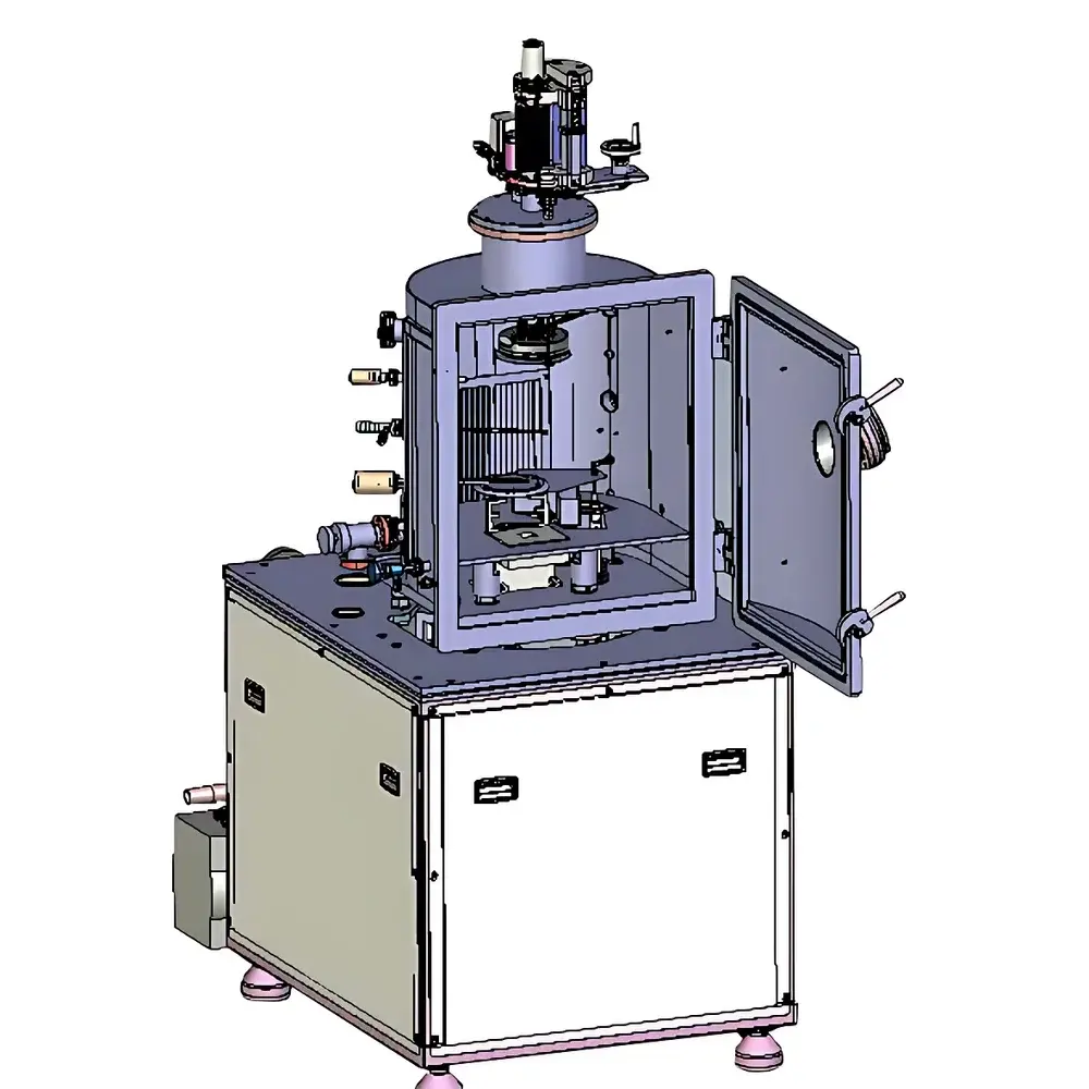
The KJ GROUP 450-Type Electron Beam Evaporation Coating System is a high-vacuum thin-film deposition platform engineered for precision physical vapor deposition (PVD) of functional inorganic and metallic thin films. Operating on the principle of electron beam-induced thermal evaporation, the system directs a focused, high-energy electron beam onto refractory target materials housed in water-cooled crucibles, achieving localized heating above 2500 °C without contaminating the vacuum environment via resistive filament degradation. This enables high-purity, stoichiometric deposition of conductive oxides (e.g., ITO, AZO), semiconductors (e.g., MoS₂ precursors, CdTe), ferroelectric perovskites (e.g., PZT, BTO), and optical interference coatings (e.g., TiO₂, SiO₂, MgF₂). Designed for research-scale reproducibility and pilot-line compatibility, the 450-Type integrates a U-shaped front-access vacuum chamber, rear-mounted turbomolecular pumping stack, and dual-mode e-gun architecture — ensuring stable beam focusing, minimal thermal drift, and long-term operational repeatability under GLP-aligned laboratory conditions.
Key Features
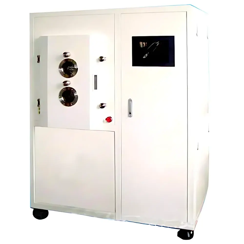
- U-shaped stainless-steel vacuum chamber (500 × 500 × 600 mm) with front hinged door and integrated O-ring sealing for rapid sample exchange and visual process monitoring
- Dual-anode electron gun (6 kV / 8 kV selectable) delivering precise beam spot control and uniform power distribution across four independent water-cooled crucibles (11 mL each)
- Programmable substrate rotation stage (5–60 rpm) with calibrated angular velocity feedback, enabling thickness uniformity better than ±3% over 4-inch substrates
- Integrated PID-controlled resistive heater with ±1 °C thermal stability at 800 °C, compatible with in-situ annealing protocols during or post-deposition
- Single-channel mass flow controller (MFC) for reactive gas introduction (O₂, N₂, Ar), supporting oxide, nitride, and oxynitride film synthesis under controlled partial pressure
- Quartz crystal microbalance (QCM) thickness monitor with sub-angstrom resolution (0.1 Å), real-time deposition rate calculation, and endpoint detection capability
- Manual shutter assembly with hardened stainless steel baffle and repeatable positioning mechanism for layer-by-layer sequential deposition
Sample Compatibility & Compliance
The 450-Type accommodates rigid planar substrates up to 100 mm (4-inch) diameter, including silicon wafers, fused silica, sapphire, glass slides, and metal foils. Its chamber geometry and source-to-substrate distance (300–350 mm) are optimized for shadow-mask-assisted patterning and multi-source co-evaporation configurations. The system complies with ISO 27427:2012 (vacuum equipment safety requirements) and meets electromagnetic compatibility (EMC) standards per IEC 61326-1. All vacuum components conform to ASTM F2789-10 (standard guide for vacuum system leak testing), and the documented leak rate (<6.7×10⁻⁷ Pa·L/s) supports qualification under ISO 14644-1 Class 5 cleanroom-adjacent operation. While not pre-certified for GMP manufacturing, its modular architecture, traceable vacuum gauging, and manual process logging interface facilitate alignment with FDA 21 CFR Part 11 data integrity expectations when paired with validated SOPs.
Software & Data Management
The system operates via a dedicated industrial PLC-based control panel with tactile push-button interface and analog metering for critical parameters (e-gun voltage/current, chamber pressure, substrate temperature, rotation speed). Real-time QCM data (thickness, rate, frequency shift) is displayed on an integrated LCD module with non-volatile memory storage (last 100 runs). For extended data capture, optional RS-232/USB export enables transfer to external lab management systems (LIMS) or MATLAB/Python-based analysis workflows. All process variables — including e-gun power ramp profiles, shutter open/close timestamps, and MFC setpoints — are logged with UTC timestamps, supporting retrospective audit trails required for GLP-compliant reporting. No cloud connectivity or proprietary software installation is required; operation remains fully deterministic and offline-capable.
Applications
- Preparation of transparent conductive oxides (TCOs) for photovoltaic device prototyping and OLED electrode development
- Growth of phase-pure ferroelectric thin films (e.g., Pb(Zr,Ti)O₃) for non-volatile memory and piezoelectric MEMS transducers
- Deposition of high-refractive-index optical coatings for laser cavity mirrors, anti-reflective stacks, and spectral filters
- Thermal evaporation of metal contacts (Au, Al, Cr, Ti) on 2D material heterostructures with minimal interdiffusion
- Reactive e-beam evaporation of compound semiconductors (e.g., ZnO:Al, CuInSe₂ precursors) under controlled oxygen partial pressure
- Multi-layer dielectric stacks for plasmonic sensor platforms and metamaterial unit cells
FAQ
What vacuum level is required for high-quality e-beam deposition of oxide films?
A base pressure ≤6.7×10⁻⁴ Pa is recommended to minimize residual gas incorporation (e.g., H₂O, CO₂) and ensure stoichiometric transfer of oxygen-sensitive compounds.
Can the system deposit multilayer structures with sharp interfaces?
Yes — the manual shutter, combined with real-time QCM feedback and stable substrate rotation, enables sequential deposition with interface roughness <0.3 nm RMS (measured by AFM post-deposition).
Is remote monitoring or automation possible?
The standard configuration supports local manual operation only; however, analog voltage outputs (0–10 V) for pressure, temperature, and thickness signals are accessible for integration into custom SCADA or LabVIEW environments.
What maintenance intervals are recommended for the e-gun and crucibles?
Crucible inspection is advised after every 50 hours of cumulative e-beam operation; e-gun filament replacement is typically required every 1,000–1,500 hours depending on operating voltage and material volatility.
Does the system support in-situ substrate biasing?
No — substrate biasing is not integrated; however, the chamber flange layout includes two CF-63 ports suitable for retrofitting RF or DC bias feedthroughs per user-defined upgrade path.


