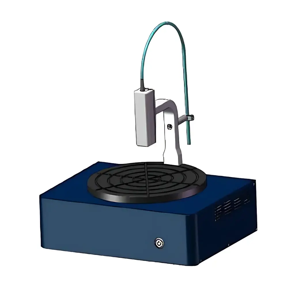
KJ GROUP CM100 Thin-Film Thickness Analyzer
| Brand | KJ GROUP |
|---|---|
| Origin | Liaoning, China |
| Manufacturer Type | Authorized Distributor |
| Country of Origin | China |
| Model | CM100 |
| Pricing | Available Upon Request |
| Spectral Range | 370–1000 nm |
| Spectral Resolution | 1.6 nm |
| Measurement Spot Size | 1.5 mm (typ.) |
| Maximum Substrate Thickness Support | 15 nm – 100 µm |
| Thickness Repeatability | ±0.1 nm |
| Max. Detectable Layers | 4 |
| Accuracy | ±2 nm or ±0.4% (whichever is greater) |
| Single-Measurement Time | 1–2 s (typ.) |
Overview
The KJ GROUP CM100 Thin-Film Thickness Analyzer is a compact, benchtop-grade spectrophotometric ellipsometer engineered for non-destructive, real-time measurement of thin-film thickness and optical constants on transparent and semi-transparent substrates. Utilizing broadband reflectance spectroscopy in the visible to near-UV range (370–1000 nm), the CM100 determines film thickness by modeling interference fringes generated at layer interfaces—principally leveraging the Fresnel equations and least-squares fitting algorithms. This physics-based approach ensures traceable, model-driven quantification without physical contact or vacuum requirements, making it suitable for routine QC in semiconductor fabrication, optical coating production, photovoltaic R&D, and academic thin-film laboratories.
Key Features
- Optimized optical path design with fixed-angle illumination (typically 65° incidence) and high-sensitivity backside-coupled CCD detector for stable spectral acquisition
- Integrated halogen-deuterium light source delivering stable intensity across the full 370–1000 nm range, calibrated against NIST-traceable standards
- Real-time spectral acquisition and automated thickness calculation with <2-second cycle time per measurement point
- Portable form factor (W × D × H: 280 × 220 × 160 mm; weight <3.2 kg) enabling deployment on cleanroom carts, glovebox-integrated workstations, or field service vehicles
- Multi-layer analysis engine supporting up to four discrete layers—including substrate, base film, interlayer, and capping layer—with simultaneous determination of thickness and refractive index (n) and extinction coefficient (k) where material dispersion models are available
- Onboard calibration routines including air-reference baseline correction and drift-compensated dark-current subtraction
Sample Compatibility & Compliance
The CM100 accommodates rigid planar samples up to 150 mm in diameter and 25 mm in thickness, including silicon wafers, fused silica, BK7 glass, ITO-coated PET, and anodized aluminum. It supports both single-layer and multi-layer stack configurations with known or pre-characterized optical dispersion relationships (e.g., Cauchy, Sellmeier, or Tauc-Lorentz models). While not certified to ISO/IEC 17025, the instrument’s measurement uncertainty budget aligns with ASTM E2375–22 (Standard Guide for Optical Interference-Based Thickness Measurements) and supports GLP-compliant documentation when paired with optional audit-trail-enabled software. All firmware and calibration data are stored internally with timestamped versioning.
Software & Data Management
The CM100 operates via KJ GROUP’s proprietary AnalytiFilm v3.2 software suite, delivered on Windows 10/11-compatible embedded PC or external host system. The interface provides live spectral preview, layer stack configuration wizard, automatic best-fit convergence diagnostics, and export of raw spectra (.csv), fit reports (.pdf), and project archives (.afp). Data files include embedded metadata: operator ID, timestamp, environmental conditions (optional USB temperature/humidity sensor input), and instrument serial number. For regulated environments, optional 21 CFR Part 11 compliance packages provide electronic signature support, role-based access control, and immutable audit trails for all measurement, calibration, and configuration events.
Applications
- Quality control of anti-reflective (AR), hard-coat, and hydrophobic films on display cover glass
- In-line thickness verification of SiO₂, SiNₓ, and Al₂O₃ ALD layers in MEMS and power device manufacturing
- R&D characterization of perovskite absorber layers and charge transport films in solar cell prototyping
- Thickness uniformity mapping across 4-inch and 6-inch wafers using motorized XYZ stage integration (optional)
- Educational use in materials science labs for teaching optical interference, thin-film optics, and parameter inversion techniques
FAQ
What substrates are compatible with the CM100?
The analyzer requires optically smooth, non-scattering substrates with measurable reflectance in the 370–1000 nm band. Common examples include silicon, quartz, sapphire, soda-lime glass, and polymer films ≥50 µm thick. Opaque or highly absorbing substrates (e.g., bulk metals without dielectric overcoats) are not supported.
Can the CM100 measure films on curved surfaces?
No. The 1.5 mm spot size and fixed optical geometry require flat, planar sample topography within ±2 µm surface deviation over the measurement area.
Is calibration required before each use?
A full factory calibration is performed prior to shipment and remains valid for 12 months under standard lab conditions (23 ±2°C, 40–60% RH). Daily verification using a supplied reference wafer (Si/SiO₂, 100 nm nominal) is recommended and takes <30 seconds.
Does the CM100 support automated stage integration?
Yes. The RS-232 and Ethernet APIs allow bidirectional communication with third-party motorized stages (e.g., Zaber, Newport) for grid-based mapping and statistical process control (SPC) reporting.
How is measurement uncertainty determined?
Uncertainty is calculated per ISO/IEC Guide 98-3 (GUM) and includes contributions from spectral noise, spot size variation, model assumption error, and environmental drift. Typical expanded uncertainty (k=2) is ±0.3 nm for 100 nm SiO₂ on Si, as documented in the included Certificate of Conformance.


