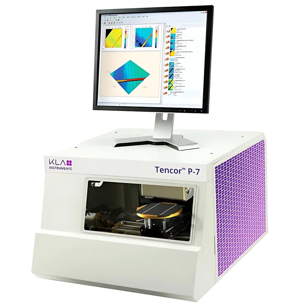
KLA P-7 Step Height Measurement System
| Brand | KLA |
|---|---|
| Origin | Malaysia |
| Manufacturer Type | Authorized Distributor |
| Origin Category | Imported |
| Model | P-7 |
| Price | USD 75,000 (FOB) |
| Measurement Principle | Capacitive Probe-Based Profilometry |
| Vertical Measurement Range | 0–1000 µm |
| Vertical Accuracy | ±0.5 Å |
| Tip Radius | 2.0 µm |
| Normal Force Range | 0.5–50 mg |
| Scan Length | 150 mm (single-pass, no stitching required) |
| Step Height Repeatability | ≤4 Å |
| Vertical Resolution | ≤0.01 Å |
| Maximum Sample Diameter | 150 mm |
| Platform Positioning Repeatability | 2 µm |
| Max Sample Height | ≥30 mm |
| Optical Zoom | 4× (motorized) |
| Camera | 5 MP color CCD |
| Digital Magnification | 4× |
| Vibration Isolation Requirement | ≤250 µin/sec (1–100 Hz) |
| Ambient Noise Limit | ≤80 dB(A) |
| Airflow Limit | ≤100 ft/min |
| Dimensions (W×D×H) | 430 × 570 × 670 mm |
| Weight | 80 kg |
Overview
The KLA P-7 Step Height Measurement System is a high-precision, contact-mode profilometer engineered for nanoscale vertical metrology in semiconductor process development, MEMS fabrication, thin-film characterization, and advanced packaging R&D. It employs a linear variable differential capacitor (LVDC) sensor architecture to deliver traceable, sub-angstrom vertical resolution and exceptional long-term stability. Unlike optical interferometric or confocal systems, the P-7 utilizes a calibrated capacitive transducer coupled with a diamond-tipped stylus—enabling direct physical interaction with surface topography while maintaining force-controlled, non-destructive scanning across diverse material classes (Si, SiO₂, photoresist, metal stacks, low-k dielectrics, and compound semiconductors). Its single-pass 150 mm scan capability eliminates stitching artifacts and preserves measurement integrity over large-area wafers and substrates, supporting both inline QC verification and offline failure analysis workflows.
Key Features
- Capacitive LVDC displacement sensing with ≤0.01 Å vertical resolution and ≤4 Å step height repeatability—validated per ISO 25178-6 and NIST-traceable calibration protocols.
- Force-regulated probe system (0.5–50 mg range) with real-time feedback control, minimizing plastic deformation on soft films and enabling reliable measurements on photoresist, polymer, and organic layers.
- Motorized 4× optical zoom with integrated 5 MP color CCD and digital magnification—facilitating precise probe positioning, defect localization, and contextual imaging without stage repositioning.
- Vacuum chuck platform with continuous 360° rotation and ±0.1° angular repeatability—supporting azimuthal profiling, edge exclusion analysis, and multi-angle cross-section extraction.
- Integrated vibration isolation compatibility: designed for operation on standard optical tables meeting ≤250 µin/sec (1–100 Hz) floor noise specifications per SEMI S2 and ISO 14644-1 Class 7 cleanroom environments.
- Automated motorized X-Y-Z stage with 2 µm positioning repeatability and programmable scan path definition—enabling batch measurement of multiple dies or test structures under identical conditions.
Sample Compatibility & Compliance
The P-7 accommodates substrates up to 150 mm in diameter and 30 mm in height, including full 150 mm wafers, diced die on tape, ceramic packages, and glass substrates. Its low-force scanning mode ensures compatibility with fragile low-k dielectrics (k < 2.7), spin-on carbon hard masks, and lithographic resists without indentation or smearing. The system complies with key industry standards for geometric metrology: ISO 25178-2 (areal surface texture), ISO 4287 (profile parameters), ASTM E1399 (step height measurement), and supports audit-ready data generation aligned with FDA 21 CFR Part 11 requirements when configured with optional electronic signature and audit trail modules. All calibration certificates are issued per ISO/IEC 17025-accredited procedures.
Software & Data Management
The KLA P-7 operates with KLA’s proprietary ProfilerSuite™ software—a Windows-based platform supporting automated recipe-driven measurement, multi-layer stack analysis, and statistical process control (SPC) charting. Raw profile data is stored in HDF5 format with embedded metadata (timestamp, operator ID, calibration status, environmental logs). Software features include cross-sectional overlay comparison, film-thickness derivation via step-height integration, curvature and wafer bow quantification (per SEMI MF1530), and stress calculation using Stoney’s equation. Export options include CSV, XML, and PDF reports compliant with internal QA documentation templates. Optional integration with factory MES systems enables direct upload of pass/fail results to centralized databases.
Applications
- Semiconductor process control: gate oxide thickness uniformity, CMP endpoint verification, etch depth monitoring, and BEOL interlayer dielectric step coverage assessment.
- MEMS and sensors: characterization of released cantilevers, comb drives, and microfluidic channel depths with sub-nanometer vertical fidelity.
- Advanced packaging: solder bump height distribution, underfill fillet geometry, and TSV (through-silicon via) recess analysis.
- Research & development: quantification of self-assembled monolayer (SAM) growth, atomic layer deposition (ALD) film conformality, and nanoscale wear track profiling.
- Failure analysis: correlation of electrical open/short failures with localized topographic anomalies such as delamination blisters or lithographic scumming.
FAQ
What sample preparation is required prior to measurement?
Minimal preparation is needed—samples must be securely mounted on the vacuum chuck with clean, flat backside contact. No conductive coating or sputtering is required, unlike electron microscopy techniques.
Can the P-7 measure transparent or highly reflective surfaces?
Yes. As a contact profilometer, it is insensitive to optical properties; measurement performance remains consistent on fused silica, sapphire, ITO-coated glass, and bare silicon.
Is thermal drift compensated during long-duration scans?
The LVDC sensor architecture provides inherent temperature stability; system-level drift is <0.05 Å/°C over 8-hour operation, verified per KLA’s thermal qualification protocol.
How is probe wear monitored and managed?
ProfilerSuite™ includes tip wear diagnostics based on signal-to-noise degradation and contact resistance trends; automatic tip replacement alerts are triggered after 500 hours of cumulative scan time or upon deviation exceeding ±2% from baseline calibration.
Does the system support GMP/GLP-compliant reporting?
When deployed with optional 21 CFR Part 11-compliant software configuration, it provides electronic signatures, immutable audit trails, and role-based access control—fully aligned with pharmaceutical and medical device manufacturing documentation requirements.