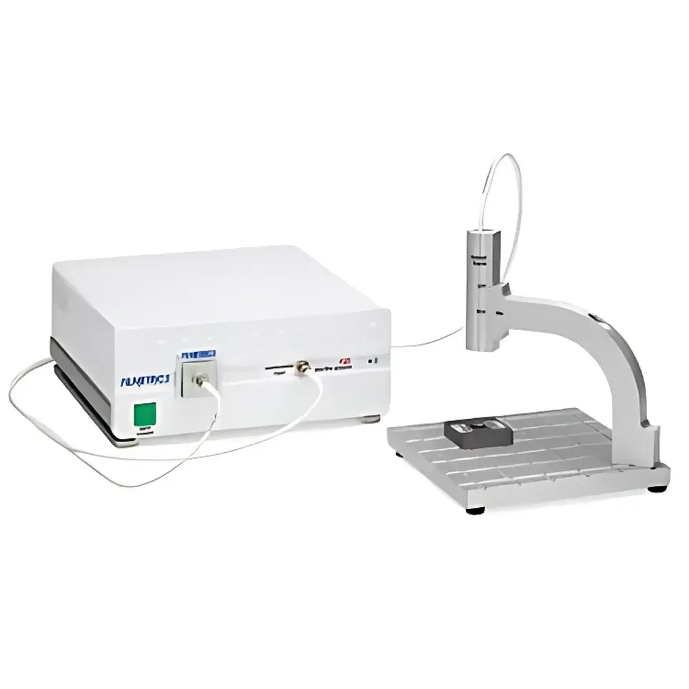
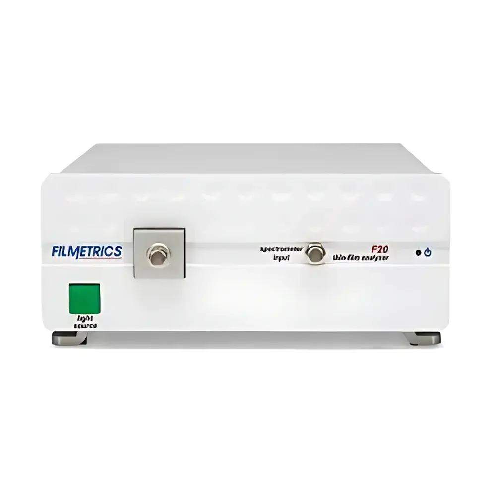
KLA Filmetrics F20 White Light Interferometric Thin-Film Thickness Measurement System
| Brand | KLA |
|---|---|
| Origin | Malaysia |
| Manufacturer Type | Authorized Distributor |
| Import Status | Imported |
| Model | F20 |
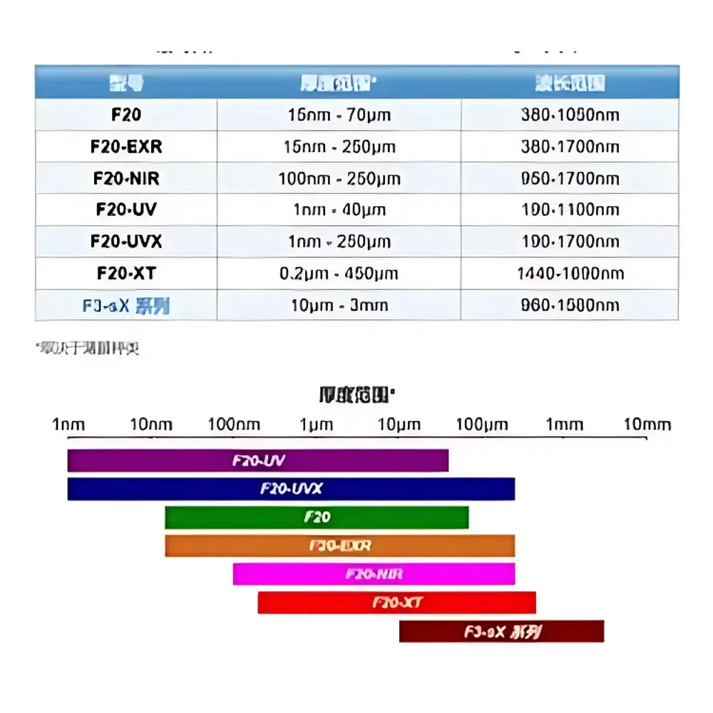
| Wavelength Range | 380–1050 nm |
| Thickness Measurement Range | 1 nm – 10 mm |
| Measurement Accuracy | ±0.02 nm |
Overview
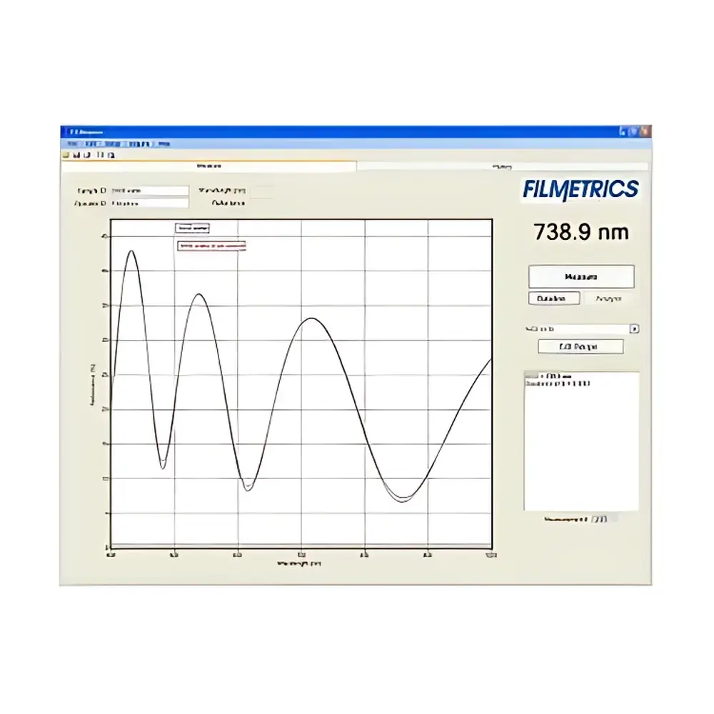
The KLA Filmetrics F20 is a benchtop white light interferometric thin-film thickness measurement system engineered for rapid, non-contact, and highly reproducible quantification of optical film thickness and refractive index (n & k). Operating on the principle of spectral reflectometry—where broadband visible-to-NIR light (380–1050 nm) is directed onto a sample surface and the interference spectrum of reflected light is analyzed via Fourier-transform-based modeling—the F20 delivers sub-angstrom resolution without requiring vacuum environments or destructive sampling. Its optical architecture leverages calibrated spectrometers, precision optics, and proprietary inverse modeling algorithms to extract thickness and dispersion data from single-layer and multilayer stacks—including absorbing semiconductors, dielectrics, polymers, and transparent conductive oxides. Designed for integration into R&D labs and pilot-line QA workflows, the F20 supports traceable measurements compliant with ISO/IEC 17025 practices and provides audit-ready metadata for GLP/GMP-aligned environments.
Key Features
- Non-destructive, contactless measurement of film thickness from 1 nm to 10 mm and refractive index across visible–NIR spectrum
- Sub-nanometer accuracy (±0.02 nm) and long-term stability (≤0.05 nm drift over 8 hours)
- Standard 1.5 mm spot size; optional micro-spot configurations down to 1 µm when integrated with user-supplied or Filmetrics-provided microscope objectives
- Automated stage compatibility for manual or robotic sample loading; supports wafer mapping up to 450 mm diameter
- Real-time spectral acquisition (<1 s per point) with full spectral data logging (380–1050 nm, 2048-pixel resolution)
- Modular hardware design: interchangeable illumination heads, fiber-coupled probes, and environmental enclosures for controlled ambient or glovebox operation
Sample Compatibility & Compliance
The F20 measures smooth, semi-transparent, or weakly absorbing films on rigid substrates—including silicon wafers, fused silica, glass, sapphire, and polymer foils. It accommodates planar and gently curved surfaces (e.g., lenses, molded optics) with radius-of-curvature down to 5 mm using optional AR-configured probes. Validated applications include photoresist, SiO₂, Si₃N₄, ITO, Al₂O₃, DLC, PI, PC, and anti-fog coatings. All measurement routines are traceable to NIST-traceable reference standards. The system supports ASTM F398 (Standard Guide for Optical Interference Thickness Measurement), ISO 9276-6 (Representation of Results of Particle Size Analysis), and USP (Optical Properties of Coatings). Data integrity complies with FDA 21 CFR Part 11 requirements when paired with Filmetrics’ optional secure software license and electronic signature module.
Software & Data Management
Filmetrics’ proprietary SpectraRay™ 4 software provides intuitive workflow-driven operation—from one-click single-point analysis to automated multi-site mapping, layer stack modeling, and time-series trend monitoring. The platform includes built-in optical constant databases (e.g., Palik, SOPRA), customizable material models (Cauchy, Sellmeier, Tauc-Lorentz), and batch processing for statistical process control (SPC). Raw spectra, fit residuals, confidence intervals, and instrument calibration logs are stored in HDF5 format for third-party analysis. Audit trails record user actions, parameter changes, and calibration events with timestamps and operator IDs. Export options include CSV, XML, and PDF reports compliant with internal QA documentation protocols.
Applications
- Semiconductor process control: photoresist development monitoring, PVD/CVD dielectric thickness uniformity, gate oxide metrology
- Optical coating QC: AR/HR coating thickness verification on lenses, filters, and laser optics
- Flexible electronics: ITO and metal mesh transparency–thickness correlation on PET and PI substrates
- Biomedical device manufacturing: hydrogel and polymer coating thickness on implantable sensors and microfluidic chips
- MEMS packaging: cavity gap and seal ring thickness assessment in hermetic encapsulation processes
- R&D validation: rapid screening of novel low-k dielectrics, 2D materials (MoS₂, h-BN), and perovskite thin films
FAQ
What substrates are compatible with the F20?
The F20 requires optically smooth, reflective or semi-transparent substrates with minimal surface roughness (<1 nm RMS). Common substrates include silicon, quartz, BK7 glass, sapphire, and polished metals with native or deposited dielectric layers.
Can the F20 measure multilayer stacks?
Yes—it supports modeling of up to 10-layer stacks with simultaneous fitting of thickness and optical constants for each layer, provided sufficient spectral contrast and known or constrained dispersion relationships.
Is vacuum or inert atmosphere required?
No—measurements are performed in ambient air. Optional purge enclosures are available for moisture- or oxygen-sensitive samples.
How is calibration maintained?
The system uses factory-calibrated spectrometer and reference mirror assemblies. Daily verification is performed using certified Si/SiO₂ step-height standards; full recalibration is recommended annually or after optical component replacement.
Does the F20 support automated production-line integration?
Yes—via Ethernet/IP or Modbus TCP interfaces, the F20 can synchronize with PLCs, SECS/GEM hosts, and MES systems for inline SPC feedback loops at up to 100 Hz sampling rate with external triggering.


