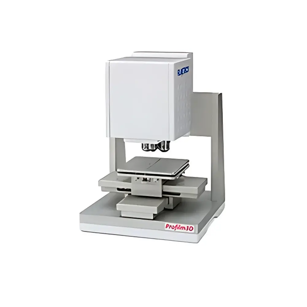
KLA Fimetrics P3D Non-Contact White-Light Interferometric Optical Profilometer
| Brand | KLA |
|---|---|
| Origin | USA |
| Model | Fimetrics P3D |
| Measurement Principle | White-Light Interferometry |
| Type | Non-Contact 3D Surface Profilometer / Roughness Analyzer |
| Key Resolution | Sub-nanometer vertical resolution (≤0.1 nm typical) |
| Field-of-View Scalability | Multi-field stitching enabled |
| Optical Configuration | Phase-shifting and vertical-scanning interferometry (CSI) |
| Compliance Basis | Designed for ISO 25178-2, ISO 4287, ASTM E1392, and VDI/VDE 2634 Part 3 |
Overview
The KLA Fimetrics P3D is a high-precision, non-contact optical profilometer engineered for quantitative 3D surface topography characterization across R&D, process development, and production environments. Based on white-light interferometry (WLI), the system implements coherent scanning interferometry (CSI) using both phase-shifting interferometry (PSI) and vertical-scanning interferometry (VSI) modalities. Unlike conventional confocal or focus-detection profilers, the P3D achieves sub-nanometer vertical resolution—typically ≤0.1 nm—without dependence on objective numerical aperture (NA), enabling consistent high-fidelity height metrology across wide fields of view (FOV) and varying surface slopes. Its dual-scan architecture allows optimal selection between PSI (for smooth, low-roughness surfaces) and VSI (for moderately rough or discontinuous topographies), ensuring measurement robustness across diverse material classes including silicon wafers, MEMS structures, optical coatings, polished metals, and biomedical substrates.
Key Features
- Sub-nanometer vertical resolution (≤0.1 nm RMS repeatability) validated per ISO 25178-6 calibration protocols
- NA-independent height sensitivity: maintains resolution integrity across magnifications from 2.5× to 100× objectives
- Automated multi-field stitching with sub-pixel registration accuracy (<0.5 µm lateral uncertainty)
- Integrated vibration-isolated granite base and active air damping for stable operation in non-lab-grade facilities
- Real-time fringe contrast optimization and adaptive focus tracking for reliable data acquisition on challenging surfaces (e.g., low-reflectivity, transparent, or highly sloped)
- Modular hardware platform supporting optional motorized Z-stage, automated XY stage, and environmental enclosure integration
Sample Compatibility & Compliance
The P3D accommodates samples up to 200 mm × 200 mm (with extended stage options), with height ranges spanning ±5 mm (standard) to ±25 mm (with extended travel). It measures surfaces with reflectivity as low as 1% (e.g., SiC, black anodized Al) and supports transparent thin films via interference-based film-thickness extraction. All measurement algorithms conform to ISO 25178-2 (areal surface texture parameters), ISO 4287 (profile-based roughness), ASTM E1392 (interferometric surface measurement), and VDI/VDE 2634 Part 3 (optical 3D measuring systems). System validation reports include traceable NIST-traceable step-height standards (e.g., 100 nm, 1 µm, 10 µm SiO₂-on-Si artifacts), and the platform supports GLP/GMP-aligned audit trails when configured with optional software modules.
Software & Data Management
The proprietary Fimetrics Analysis Suite provides intuitive workflow-driven operation—from rapid one-click profiling to advanced scriptable analysis. The software includes ISO-compliant parameter calculation (Sa, Sq, Sz, Sdr, Vmp, etc.), cross-section extraction, curvature mapping, defect detection with customizable thresholds, and statistical process control (SPC) charting. Raw interferogram data is stored in vendor-neutral HDF5 format with embedded metadata (wavelength, objective, scan settings, calibration ID). For regulated environments, optional FDA 21 CFR Part 11 compliance packages provide electronic signatures, role-based access control, and immutable audit logs covering user actions, parameter edits, and report generation events.
Applications
- Wafer-level metrology: CMP uniformity, etch depth monitoring, lithography overlay verification
- MEMS/NEMS device characterization: actuator displacement, membrane deflection, stiction analysis
- Optics manufacturing: lens surface form error, coating thickness uniformity, scratch/defect quantification
- Medical device QA: stent strut geometry, implant surface texturing, microfluidic channel depth profiling
- Advanced packaging: solder bump coplanarity, underfill void analysis, TSV inspection
- Academic research: thin-film growth kinetics, corrosion morphology evolution, tribological wear track quantification
FAQ
What surface materials can the P3D measure reliably?
It supports conductive (Si, Cu, Au), dielectric (SiO₂, Si₃N₄, glass), polymeric (PMMA, PDMS), and biological (collagen scaffolds, cell monolayers) surfaces—provided minimal coherence noise and sufficient fringe contrast are maintained.
Does the system require environmental control?
While not mandatory, temperature stability within ±1°C/hour and low-air-turbulence conditions are recommended for sub-nanometer repeatability; optional climate enclosures are available for production-floor deployment.
Can the P3D export data to third-party analysis tools?
Yes—surface maps are exportable as ASCII XYZ, CSV, or standard image formats (TIFF, PNG); full interferogram stacks support MATLAB and Python (via h5py) ingestion.
Is calibration traceable to national standards?
All factory calibrations use NIST-traceable step-height standards, with certificate documentation provided per ISO/IEC 17025 guidelines.
How does the P3D handle steep slopes or overhangs?
Vertical-scanning mode (VSI) enables reliable measurement of slopes up to 70°; for extreme topographies (>85°), hybrid workflows combining WLI with complementary techniques (e.g., confocal or SEM) are advised.