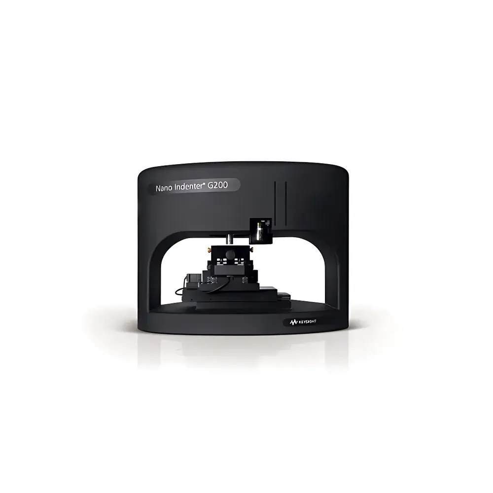
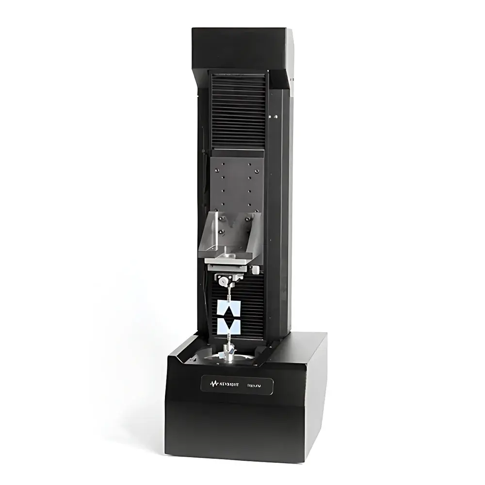
KLA K-T G200 / I-Nano / Insitu In-Situ Nanomechanical Testing System
| Brand | KLA |
|---|---|
| Origin | USA |
| Model | K-T G200 / I-Nano / Insitu |
| Application | In-situ nanomechanical characterization with optical, electrical, and structural correlation |
Overview
The KLA K-T G200 / I-Nano / Insitu In-Situ Nanomechanical Testing System represents the culmination of over three decades of innovation in quantitative nanoscale mechanical metrology. Engineered for precision and reproducibility, this platform implements the patented Continuous Stiffness Measurement (CSM) technique—now codified in ISO 14577-1:2015 and ASTM E2546–18—as its foundational method for depth-sensing indentation. Unlike conventional quasi-static indentation, CSM superimposes a small oscillatory force (typically 2–10 nm amplitude, 45–100 Hz frequency) onto the primary loading ramp, enabling real-time, high-resolution tracking of contact stiffness, elastic modulus, hardness, and viscoelastic response during loading, unloading, and dwell phases. The system is uniquely configured for true in-situ operation: integrated stages, environmental chambers, and synchronized interfaces allow concurrent mechanical testing inside scanning electron microscopes (SEM), transmission electron microscopes (TEM), optical microscopes, and electrical probe stations—enabling direct correlation between nanomechanical behavior and evolving microstructure, phase transformation, or local conductivity.
Key Features
- Patented Continuous Stiffness Measurement (CSM) compliant with ISO 14577 and ASTM E2546 for dynamic modulus and hardness mapping at sub-10 nm depth resolution
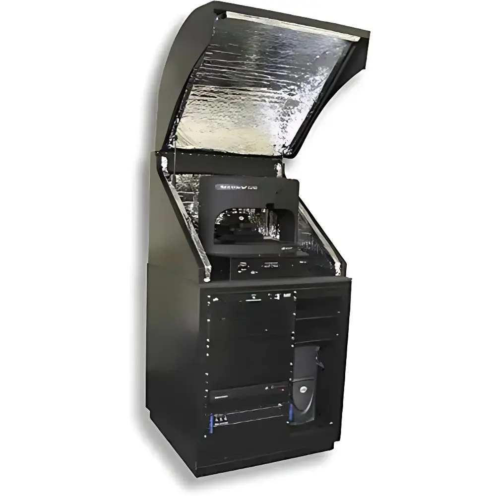
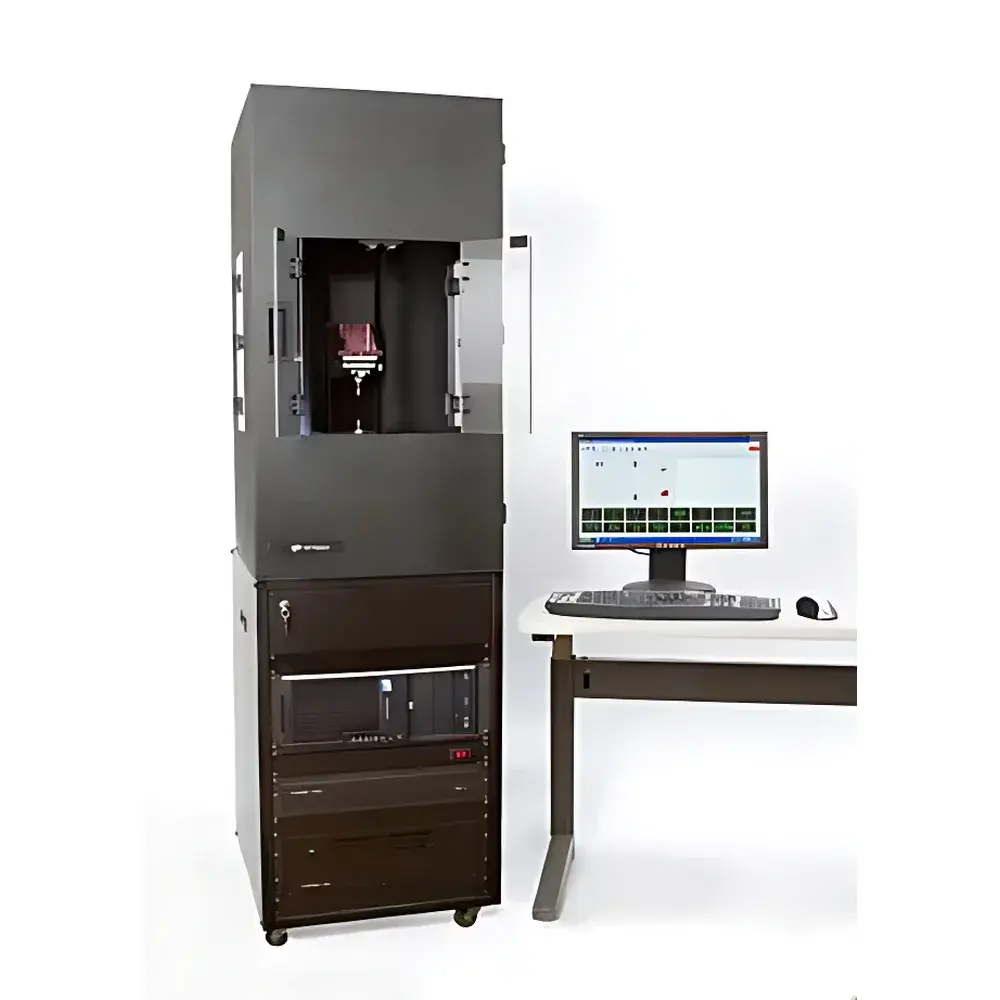
- Modular architecture supporting three core configurations: K-T G200 (high-force, macro-to-nano scale), I-Nano (ultra-high-resolution, low-force <100 µN), and Insitu (dedicated SEM/TEM-compatible stage with sub-50 nm positional repeatability)
- Sub-nanometer displacement resolution (≤0.05 nm) and force resolution down to 30 nN, calibrated traceably to NIST standards
- Integrated high-speed imaging synchronization (via TTL triggers and frame-grabber interfaces) for simultaneous acquisition of load-displacement curves and real-time SEM/TEM video streams
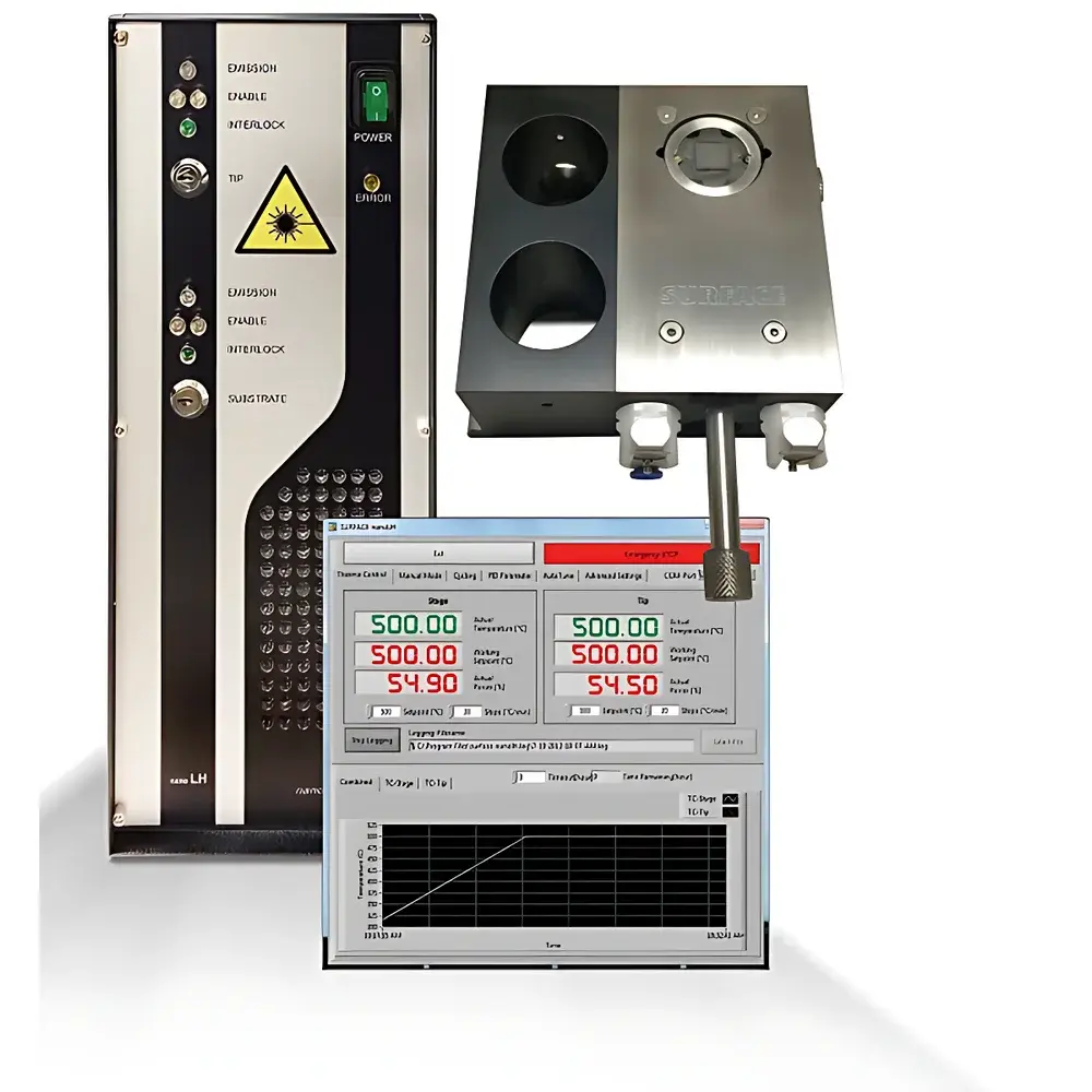
- Motorized XYZ stages with closed-loop piezoelectric actuators, enabling automated grid-based nanoindentation, scratch profiling, and fatigue cycling under controlled thermal or gaseous environments
- Robust mechanical design optimized for vibration isolation and long-term stability in shared microscopy facilities
Sample Compatibility & Compliance
The K-T G200 / I-Nano / Insitu accommodates a broad range of solid-state specimens—including single-crystal metals, thin-film coatings (e.g., DLC, TiN, Al₂O₃), semiconductor heterostructures, polymer blends, biomaterials, and geological minerals—without requiring conductive coating for SEM-compatible testing. All configurations meet electromagnetic compatibility (EMC) requirements per EN 61326-1 and safety standards per IEC 61010-1. Data integrity and audit readiness are ensured through optional FDA 21 CFR Part 11-compliant software modules, including electronic signatures, user role-based access control, and immutable audit trails for GLP/GMP-regulated environments.
Software & Data Management
Operation is governed by TriboScan™ v5.x, a modular, scriptable platform supporting both guided workflows and advanced customization via Python API. Real-time data visualization includes live load-displacement loops, modulus/hardness maps overlaid on SEM images, and time-resolved creep/recovery plots. Raw data is stored in HDF5 format with embedded metadata (instrument configuration, calibration history, environmental conditions), ensuring FAIR (Findable, Accessible, Interoperable, Reusable) compliance. Export options include ASCII, MATLAB .mat, and standardized MDF (Materials Data Format) for integration into institutional materials informatics pipelines.
Applications
- Quantitative evaluation of interfacial adhesion and delamination kinetics in multilayer thin-film systems
- In-situ observation of dislocation nucleation, pile-up evolution, and crack initiation in crystalline materials under mechanical loading
- Mechanical property gradients across grain boundaries, phase boundaries, and irradiation-damaged zones in nuclear materials
- Time-dependent deformation behavior (creep, stress relaxation) of soft matter and hydrogels under physiological temperature and humidity
- Correlative nanomechanics-electrical transport studies in 2D materials (e.g., MoS₂, graphene) and perovskite solar cell layers
- Validation of multiscale finite element models using experimentally derived local constitutive parameters
FAQ
Is the system compatible with field-emission SEMs and cryo-TEMs?
Yes—the Insitu configuration includes UHV-rated feedthroughs, differential pumping options, and compact kinematic mounting to support integration with FE-SEM columns and dedicated cryo-TEM holders.
Can CSM data be exported for third-party modeling tools like ABAQUS or COMSOL?
Absolutely—TriboScan™ supports direct export of calibrated force-displacement datasets with time-stamped metadata, enabling seamless import into commercial FEA platforms for inverse modeling and parameter identification.
Does the system support automated tip certification and area function verification?
Yes—integrated reference standard routines execute ISO 14577 Annex B-compliant tip geometry verification using fused silica and sapphire calibration samples, with automated area function fitting and drift correction.
What level of technical support is available outside North America?
KLA maintains regional service centers in Shanghai, Tokyo, and Munich, staffed by application engineers certified in nanomechanics metrology and trained directly at the US R&D facility in Milpitas, CA. On-site installation, qualification (IQ/OQ/PQ), and annual recalibration services are available globally.


")
