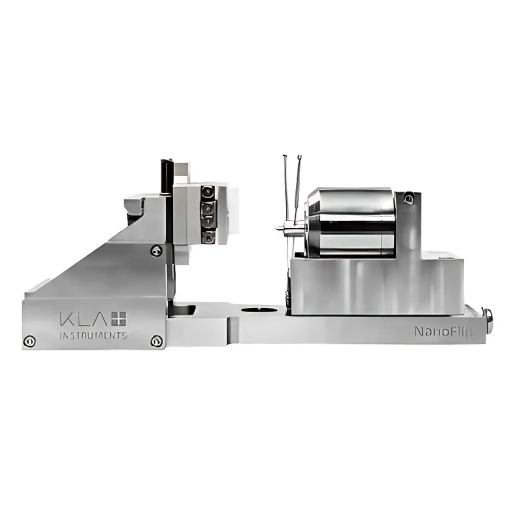
KLA NanoFlip In-Situ Nanomechanical Testing System
| Brand | KLA |
|---|---|
| Origin | USA |
| Model | NanoFlip |
| Instrument Type | Integrated Nanoindentation and Scratch Tester |
| Environmental Operation | Vacuum and Controlled Atmosphere (including Glovebox-Compatible) |
| Actuator | InForce 50 Electromagnetic Force Actuator with Capacitive Displacement Sensing |
| Controller | InQuest High-Speed Digital Controller (100 kHz Data Acquisition, 20 µs Time Constant) |
| Motion System | Motorized XYZ Stage (X/Y: 21 mm Travel, Z: 25 mm Travel) |
| Sample Orientation | Flip Mechanism for SEM/FIB Imaging Alignment |
| FIB-to-Test Capability | 90° Sample Tilt for Seamless Transition from FIB Milling to Nanomechanical Testing |
| Software | InView™ v6.x (Windows® 10 Compatible), Includes ISO 14577 Compliance Module, User Method Development Toolkit, Real-Time SEM Video Synchronization, Integrated Tip Calibration Suite |
Overview
The KLA NanoFlip In-Situ Nanomechanical Testing System is an engineered solution for quantitative, high-resolution mechanical characterization at the nanoscale under real-time imaging conditions. Built upon the principles of instrumented nanoindentation—governed by contact mechanics theory and calibrated via the Oliver-Pharr method—the NanoFlip enables direct correlation between structural morphology and localized mechanical response. Its core architecture integrates a high-bandwidth electromagnetic actuator (InForce 50), capacitive displacement sensing, and a motorized triaxial positioning system, allowing precise control of load, displacement, and spatial registration within scanning electron microscopes (SEM), focused ion beam (FIB) systems, or inert-atmosphere gloveboxes. Unlike conventional ex-situ testers, the NanoFlip’s flip-stage design permits rapid reorientation of the sample between imaging and testing axes without manual intervention or realignment, minimizing drift and preserving positional fidelity. This capability is critical for iterative workflows such as FIB-based micropillar fabrication followed immediately by uniaxial compression, or in situ observation of pop-in events during indentation into crystalline lattices.
Key Features
- InForce 50 electromagnetic actuator with sub-nanometer displacement resolution and <1 nN force noise floor, enabling stable operation in vacuum (<10⁻⁶ Torr) and reactive gas environments.
- InQuest digital controller supporting 100 kHz data acquisition and 20 µs time constant for capturing transient deformation phenomena—including displacement bursts, creep relaxation, and viscoelastic recovery.
- Fully motorized XYZ stage with 21 mm × 21 mm lateral travel and 25 mm vertical range, facilitating large-area mapping across heterogeneous samples and multi-height topographies.
- Integrated flip mechanism enabling 90° sample rotation for seamless transition between FIB milling and nanoindentation, eliminating sample remounting and preserving fiducial alignment.
- Real-time synchronization of SEM video streams with force–displacement data via InView software, supporting frame-accurate overlay of mechanical events on microstructural features.
- Onboard tip calibration routine embedded in InView, compliant with ISO 14577 Annex B, reducing setup time and improving inter-laboratory reproducibility.
- Windows® 10–compatible InView platform with built-in test protocols (CSM, ISO 14577, NanoBlitz, AccuFilm™, ProbeDMA™), plus optional User Method Development toolkit for custom script-based experiments.
Sample Compatibility & Compliance
The NanoFlip accommodates specimens ranging from ultra-soft hydrogels (E 300 GPa), using interchangeable tips including Berkovich, cube-corner, Vickers, spherical, flat-punch, and conical geometries. All tip calibrations are traceable to NIST-traceable reference standards, and system-level verification follows ASTM E2546 and ISO 14577-1:2016 requirements. For regulated environments, InView supports audit trails, electronic signatures, and 21 CFR Part 11–compliant data integrity features when configured with GLP/GMP modules. The system meets CE marking requirements for electromagnetic compatibility (EMC) and low-voltage directive compliance. Environmental flexibility extends to inert-gas gloveboxes (Ar/N₂), high-vacuum SEM chambers (≤10⁻⁷ mbar), and controlled-humidity stages—ensuring consistent performance across academic, industrial R&D, and quality assurance settings.
Software & Data Management
InView software serves as the unified interface for experiment design, execution, and post-processing. It provides native support for continuous stiffness measurement (CSM), dynamic mechanical analysis (DMA), and high-throughput mapping modes such as NanoBlitz 3D/4D. Data export conforms to HDF5 and ASCII formats, ensuring interoperability with MATLAB®, Python (NumPy/Pandas), and commercial statistical packages. All raw datasets include metadata tags for instrument configuration, environmental conditions, tip geometry, and calibration history—enabling FAIR (Findable, Accessible, Interoperable, Reusable) data practices. Optional DataBurst mode captures displacement transients at >1 kHz sampling rates, essential for analyzing dislocation nucleation, phase transformation onset, or interfacial delamination kinetics. The User Method Development toolkit allows scripting in Python-like syntax, empowering researchers to implement conditional logic, adaptive loading sequences, or closed-loop feedback control—capabilities validated in peer-reviewed publications on metallic glass deformation and battery electrode fracture.
Applications
The NanoFlip addresses fundamental and applied challenges across advanced materials science. In MEMS development, it quantifies residual stress gradients and interfacial adhesion in thin-film stacks subjected to thermal cycling. In battery research, it maps modulus evolution across SEI layers during electrochemical cycling inside operando cells. For nuclear materials, it evaluates irradiation-induced hardening in zirconium alloys using in vacuo pillar compression. In polymer nanocomposites, ProbeDMA™ enables frequency-swept nano-DMA to resolve glass transition breadth and filler-matrix coupling effects inaccessible to bulk DMA. In semiconductor packaging, AccuFilm™ isolates intrinsic film properties from substrate contributions in low-k dielectrics and Cu diffusion barriers. Additional use cases include quantitative scratch testing of anti-reflective coatings, wear track profiling of biomedical implants, and mechanical phenotyping of tissue-engineered scaffolds.
FAQ
Does the NanoFlip support ISO 14577-compliant hardness testing?
Yes—InView includes preconfigured ISO 14577 test templates that automatically compute instrumented hardness, reduced Young’s modulus, Vickers-equivalent hardness, and normalized indentation work, with full traceability to calibration certificates.
Can the system perform tests inside a scanning electron microscope?
Yes—the NanoFlip is designed for direct integration into SEM and dual-beam FIB-SEM platforms, with compact footprint (<200 mm × 200 mm base), EMI-shielded cabling, and vacuum-compatible materials.
Is tip calibration automated?
Yes—an integrated software-guided calibration sequence uses reference samples and geometric algorithms to determine tip area function and frame compliance, eliminating manual probe characterization steps.
What is the maximum achievable data rate during indentation?
With DataBurst enabled, displacement data can be recorded at up to 2 MHz; standard CSM and quasi-static modes operate at 100 kHz with synchronized force and displacement channels.
How does FIB-to-Test functionality improve experimental throughput?
By rotating the sample 90° within the same chamber, users avoid breaking vacuum or relocating fiducials—reducing total cycle time per site from ~45 minutes to under 5 minutes while maintaining sub-100 nm positional repeatability.


