kSA MOS In-Situ Thin Film Stress Measurement System
| Brand | k-Space Associates |
|---|---|
| Origin | USA |
| Model | kSA MOS |
| Stress Measurement Range | 0.32 MPa – 7.8 GPa |
| Measurement Technology | Multi-Beam Optical Sensor (MOS) |
| Operating Temperature | Ambient to system process temperature (vacuum chamber compatible) |
| Compliance | Designed for UHV/MBE/MOCVD integration, vacuum-rated optical interface, ISO 9001-manufactured instrumentation |
Overview
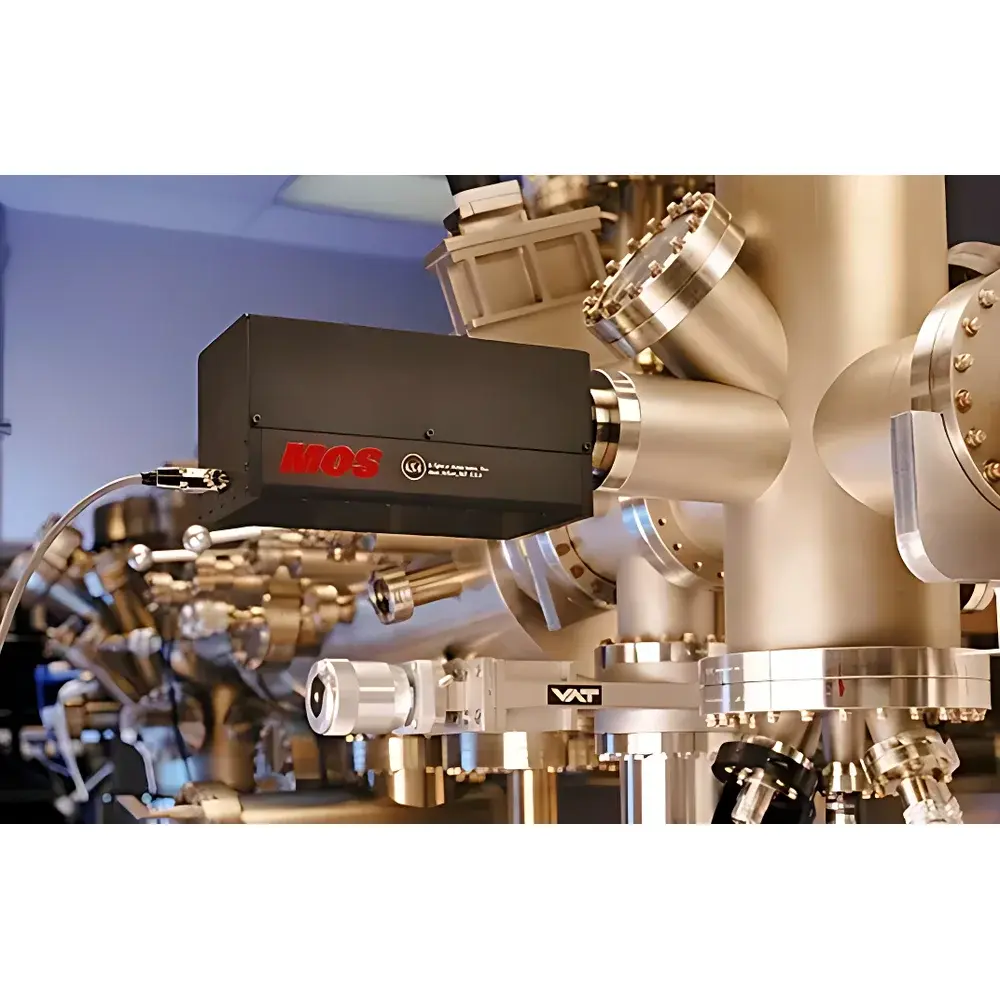
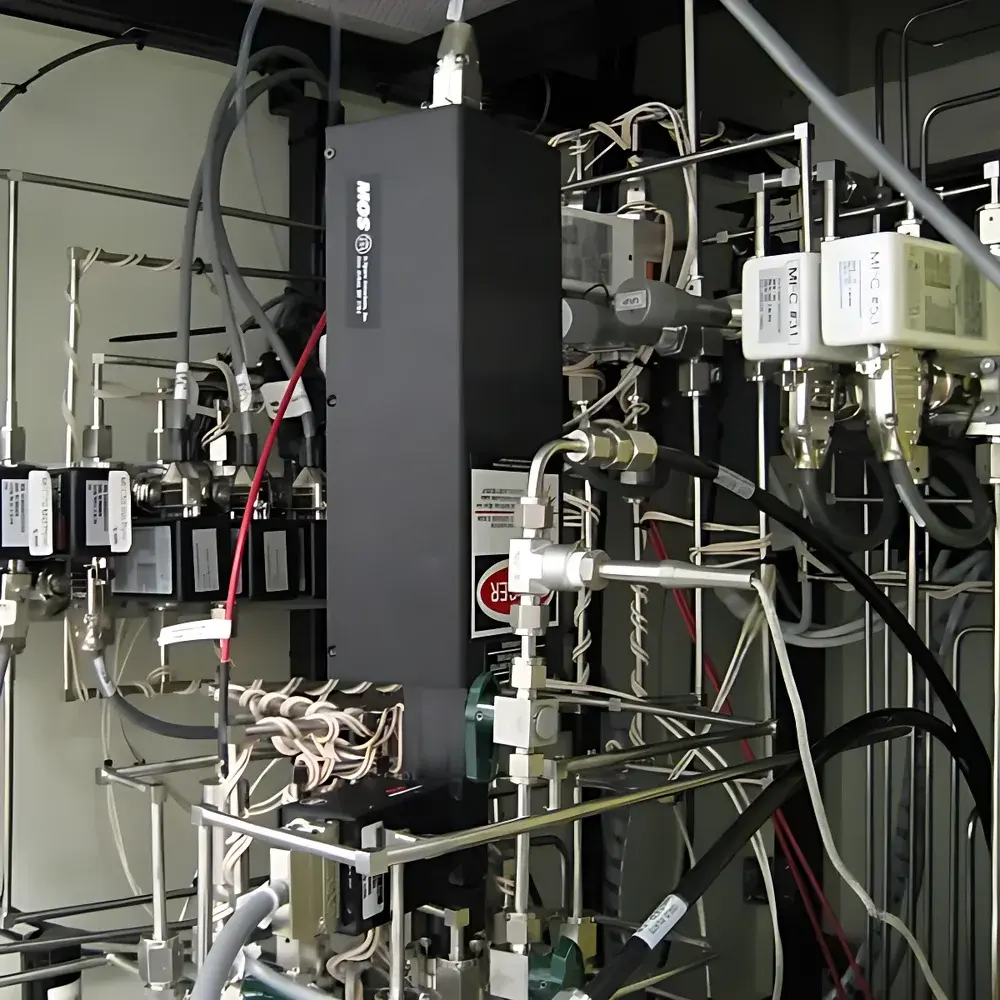
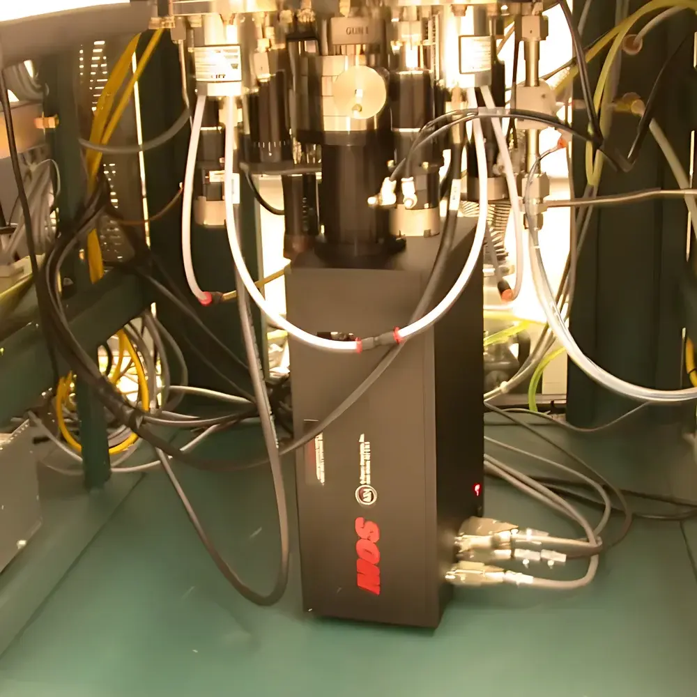
The kSA MOS In-Situ Thin Film Stress Measurement System is an engineered solution for real-time, non-contact quantification of mechanical stress and curvature evolution during thin film growth and thermal processing. Based on the patented Multi-Beam Optical Sensor (MOS) technology (U.S. Patent No. 7,391,523 B1), the system operates on the Stoney equation principle—deriving biaxial stress from substrate curvature change measured via high-resolution laser beam deflection arrays. Unlike single-point interferometric or wafer-bow methods, the kSA MOS employs a synchronized multi-laser configuration (typically 3×3 or customizable grid) that scans coherently across the substrate surface, enabling true 2D stress mapping with sub-microradian angular resolution. Its design eliminates sensitivity to external mechanical vibration—a critical requirement in ultra-high-vacuum (UHV) environments such as molecular beam epitaxy (MBE), metalorganic chemical vapor deposition (MOCVD), sputtering, pulsed laser deposition (PLD), and rapid thermal processing (RTP) systems. The instrument integrates directly through a single top port or dual symmetric ports, maintaining full compatibility with standard vacuum flanges (CF, KF, ISO-K) and process chamber geometries.
Key Features
- Patented Multi-Beam Optical Sensor (MOS) technology for simultaneous, vibration-immune curvature acquisition across up to 9 discrete measurement points
- Real-time calculation of biaxial stress (MPa–GPa range), radius of curvature (mm–m), and stress-thickness profiles during film deposition or annealing
- Configurable laser point selection: users define active measurement zones—single spot, linear scan, or full 2D grid—without hardware reconfiguration
- Vacuum-compatible optical head rated for pressures down to 1×10⁻¹⁰ Torr; no internal moving parts or consumables
- Native support for anisotropic stress analysis via directional curvature gradient evaluation
- Optional add-ons include in-situ growth rate monitoring (via reflectance oscillation analysis), optical constants (n & k) extraction (spectroscopic reflectometry module), multi-wafer capability (carousel-compatible), and substrate rotation tracking (for radial uniformity assessment)
- Real-time optical feedback loop enables closed-loop process control integration (e.g., shutter timing adjustment based on stress threshold crossing)
Sample Compatibility & Compliance
The kSA MOS system supports substrates ranging from 25 mm to 150 mm diameter—including Si, GaAs, sapphire, SiC, quartz, and flexible metallic foils—with no minimum thickness restriction. It accommodates films from monolayer-scale 2D materials (e.g., MoS₂, graphene) to thick (>10 µm) dielectric stacks. All optical components meet RoHS and REACH directives. The system architecture conforms to industrial vacuum safety standards (SEMI F27, ISO 27401) and supports audit-ready data logging compliant with GLP and GMP frameworks. While not FDA-certified per se (as a research-grade metrology tool), its timestamped, uneditable measurement logs—including raw deflection voltages, calibrated curvature values, and user-defined metadata—meet foundational requirements for 21 CFR Part 11 electronic record integrity when deployed with validated IT infrastructure.
Software & Data Management
Control and analysis are executed via kSA’s proprietary MOSView™ software suite (Windows-based, 64-bit). The application provides synchronized visualization of curvature, stress, and thickness evolution with configurable time-resolution (down to 10 ms per frame). Data export formats include CSV, HDF5, and MATLAB (.mat) for post-processing interoperability. Built-in scripting (Python API) allows automated sequence execution, alarm triggering, and integration with PLCs or recipe management systems. All measurement sessions generate immutable audit trails containing operator ID, system calibration timestamps, environmental logs (chamber pressure, temperature), and version-stamped firmware/software identifiers—ensuring traceability for academic publication or process qualification documentation.
Applications
The kSA MOS system serves as a core metrology platform in semiconductor R&D, compound semiconductor manufacturing, MEMS development, and advanced packaging. It is routinely deployed to characterize strain relaxation kinetics in lattice-mismatched heterostructures (e.g., InGaAs on InP), quantify thermal stress hysteresis in Cu/low-k interconnect stacks, monitor stress-driven cracking in piezoelectric AlN films, and validate stress-engineering strategies in strained-Si CMOS processes. Academic labs use it to correlate stress evolution with surface morphology (in situ with RHEED or AFM), while industrial users leverage its stability for process window definition, tool matching studies, and yield correlation analysis across cluster tools.
FAQ
Can the kSA MOS measure stress in amorphous or polycrystalline films?
Yes—the MOS technique relies solely on substrate curvature deformation and does not require crystallinity, making it equally applicable to amorphous SiO₂, poly-Si, or metallic thin films.
Is calibration required before each run?
No—factory calibration is retained across power cycles. Optional daily verification using a certified reference wafer (NIST-traceable curvature standard) is recommended for ISO 17025-compliant labs.
Does the system support cryogenic or high-temperature measurements?
Yes—operation is defined by the host chamber’s thermal envelope; the optical head maintains functionality from 10 K (with optional LN₂-cooled viewport) to >1000 °C (using high-temp quartz windows and thermal shielding).
How is data synchronization handled with other in-situ tools (e.g., RHEED, QCM)?
Via TTL trigger I/O and shared timebase referencing; MOSView supports hardware-synchronized acquisition with third-party instruments using common clock distribution.
What vacuum feedthrough options are available?
Standard configurations include CF-63, CF-100, and ISO-K 160 flanges; custom viewports with anti-reflective coatings or UV-transmissive fused silica are available upon request.


