Laue Crystal Orientation Mapping System
| Origin | UK |
|---|---|
| Manufacturer Type | Distributor |
| Origin Category | Imported |
| Model | Laue System |
| Price Range | USD 42,000 – 70,000 |
Overview
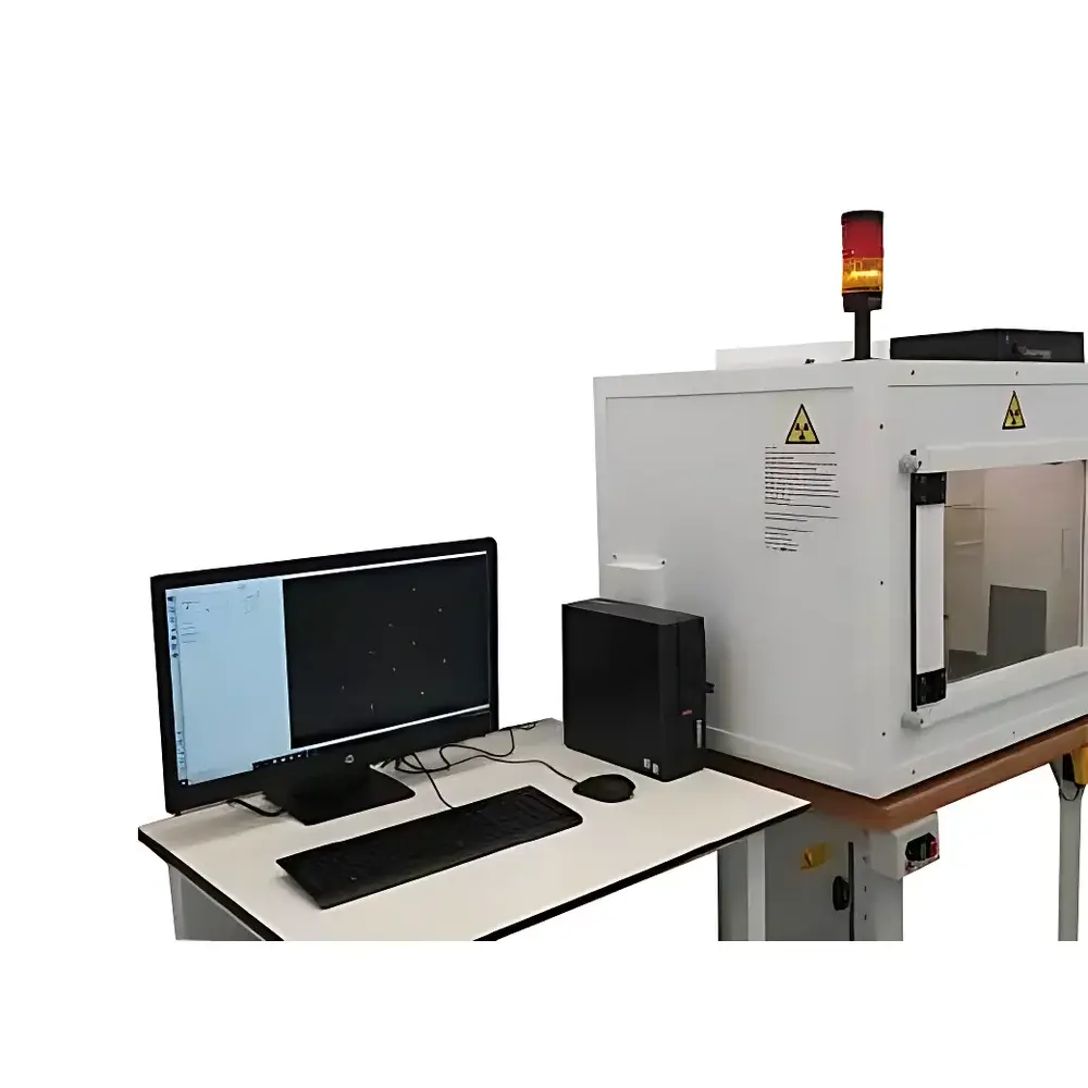
The Laue Crystal Orientation Mapping System is a high-precision X-ray diffraction instrument engineered for rapid, non-destructive determination of crystallographic orientation in single crystals and polycrystalline materials. Based on back-reflection Laue diffraction geometry, the system utilizes a white (polychromatic) X-ray beam incident on a stationary crystal to generate a characteristic spot pattern on a large-area CCD detector. Each diffraction spot corresponds to a specific reciprocal lattice vector, enabling full three-dimensional orientation matrix reconstruction via geometric indexing. Designed for industrial R&D labs and academic crystal growth facilities, the system delivers angular resolution down to 0.05° (RMS) with traceable calibration against NIST-traceable reference standards. Its modular architecture supports both horizontal and vertical sample configurations—optimized respectively for heavy (>20 kg) bulk ingots and thin wafers or small-grain polycrystals.
Key Features
- Back-reflection Laue geometry with <200 µm focused X-ray beam—enabling high-resolution orientation mapping of sub-millimeter crystals
- Dual-mode positioning: motorized goniometer (±0.02° repeatability) for precision alignment; manual fine-tuning compatible with cutting tools and synchrotron/neutron beamline interfaces
- High-dynamic-range PSEL CCD detector: 1867 × 1265 pixel array, 83 µm effective pixel size, active area 155 × 105 mm²
- Flexible exposure control: 1 ms to 35 min integration time; on-chip pixel binning for SNR optimization; automatic background subtraction
- Two acquisition modes: 16-bit high-precision mode for quantitative analysis; 12-bit fast preview mode for real-time alignment
- Integrated laser distance sensor and coaxial video monitoring camera for fiducial-based sample registration and drift compensation
Sample Compatibility & Compliance
The system accommodates diverse sample geometries—from 2-inch semiconductor wafers to 300 mm diameter silicon ingots and cylindrical rods up to 500 mm in length. Horizontal configuration supports samples weighing up to 25 kg; vertical configuration enables large-area wafer mapping and multi-sample batch processing. All mechanical stages comply with ISO 9283 repeatability standards. Software workflows support GLP-compliant data integrity: audit trails, electronic signatures, and CSV-exported orientation matrices with timestamping and operator ID—fully aligned with FDA 21 CFR Part 11 requirements for regulated environments. Calibration routines are traceable to SI units via certified reference crystals (e.g., Si, Cu, α-Al₂O₃).
Software & Data Management
Powered by PSEL’s Python-based Laue Analysis Suite, the software provides end-to-end workflow automation—from raw image acquisition to orientation matrix export. Key modules include: (1) Auto-spot detection using adaptive thresholding and Hough transform-based indexing; (2) Real-time orientation error calculation relative to user-defined crystallographic axes without manual distortion correction; (3) Batch processing for wafer-scale 2D orientation mapping with interpolation and grain boundary identification; (4) Remote operation via TCP/IP socket interface—enabling integration into factory MES or synchrotron control systems. All measurement metadata—including beam parameters, stage positions, exposure settings, and calibration logs—are embedded in TIFF/CSV outputs. Raw images retain full 16-bit depth for retrospective reprocessing.
Applications
The system serves critical quality control and process development functions across advanced materials sectors: semiconductor substrates (SiC, AlN, InP), infrared detector materials (HgCdTe/CdTe, InSb, InGaAs), piezoelectric/ferroelectric ceramics (LiNbO₃, quartz, PZT), laser gain media (Nd:YAG, KTP, GaAs), high-temperature superconductors (YBCO, BSCCO), magnetic oxides (FeSe, NiO), scintillation crystals (LYSO, BGO, CdWO₄), and refractory metal alloys (W, Mo, Ni-based superalloys). It is routinely deployed for seed crystal verification, epitaxial layer alignment, wafer slicing angle optimization, and post-growth strain mapping.
FAQ
What crystal symmetry classes can the software automatically index?
The PSEL software supports all 32 crystallographic point groups and handles centrosymmetric/non-centrosymmetric lattices—including triclinic, monoclinic, orthorhombic, tetragonal, hexagonal, rhombohedral, and cubic systems—using a robust lattice parameter refinement engine.
Is the system compatible with third-party X-ray sources?
Yes—the detector and software accept TTL-synchronized external triggers and support standard X-ray generator interfaces (e.g., Rigaku, Bruker, custom microfocus tubes) via programmable HV control and shutter signals.
Can orientation data be exported to CAD or crystal growth simulation tools?
Orientation matrices are exported in Euler angle (ZXZ convention), rotation quaternion, and axis-angle formats; CSV files include column headers compliant with Thermo Fisher Avizo, MATLAB, and COMSOL Multiphysics import protocols.
Does the system meet ISO/IEC 17025 calibration requirements?
Yes—calibration certificates include uncertainty budgets per GUM (JCGM 100:2008), covering angular accuracy, beam divergence, and detector spatial linearity; optional on-site metrology services available through UKAS-accredited partners.


