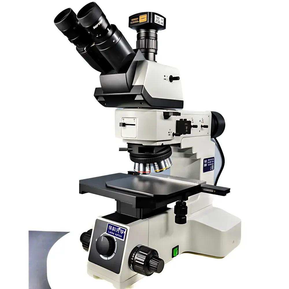

LEI-TECH LK-63R UISC Infinite Conjugate Metallurgical Microscope
| Brand | LEI-TECH |
|---|---|
| Origin | Tianjin, China |
| Manufacturer Type | OEM Manufacturer |
| Product Type | Upright |
| Image Analysis System | Integrated |
| Total Magnification Range | 50×–1000× |
| Eyepiece | PL10×/22 mm Widefield High-Eyepoint |
| Objective Lenses | 5×, 10×, 20×, 50×, 100× (Long Working Distance, Semi-Apochromatic, Brightfield/Darkfield Dual-Mode) |
| Optical System | UISC (Universal Infinite Space Correction) Infinity-Corrected Optics |
| Illumination | Reflected 12 V / 100 W Halogen with Digital Intensity Preset & BF/DF Toggle |
| Observation Modes | Brightfield (BF), Darkfield (DF), Differential Interference Contrast (DIC), Simple Polarization |
| Stage | 6-inch (158 × 158 mm XY travel under reflected light |
| Focus Mechanism | Coaxial Coarse/Fine Adjustment with Upper Limit Stop & Tension Control |
| Power Supply | Built-in 90–240 V AC Universal Voltage Transformer |
| Camera Interface | C-mount, Compatible with 20 MP (5440 × 3648) Digital Imaging Module |
Overview
The LEI-TECH LK-63R is an upright metallurgical microscope engineered for high-precision microstructural analysis in semiconductor wafer inspection, failure analysis, metallography, and advanced materials characterization. It implements a proprietary UISC (Universal Infinite Space Correction) optical architecture—an infinity-corrected system that decouples objective and tube lens functions to enable modular expansion, consistent aberration control across magnifications, and compatibility with auxiliary contrast modules including DIC prisms and polarization optics. Unlike finite-conjugate systems, the UISC design ensures minimal chromatic and spherical distortion, uniform illumination intensity across the field of view, and stable parfocality when switching objectives or adding optical components. The LK-63R’s rigid cast-metal frame, low-center-of-gravity chassis, and internal forced-air thermal management ensure mechanical stability during extended imaging sessions—critical for automated metrology workflows and long-duration SEM correlation studies.
Key Features
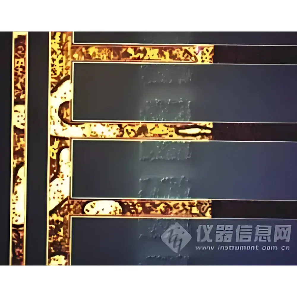
- UISC Infinity-Optimized Optics: Fully corrected semi-apochromatic objectives (5×–100×) featuring multi-layer broadband anti-reflection coatings and extended working distances (7.8 mm at 50×, 2.1 mm at 100×), enabling safe observation of tall or topographically complex specimens such as solder bumps, MEMS structures, and coated wafers.
- Dual-Mode Illumination Architecture: Independent control of reflected (12 V / 100 W halogen, digitally presettable intensity, centerable field diaphragm) and transmitted (5 W white LED, NA 0.5 Abbe condenser) light paths allows simultaneous BF/DF illumination or sequential mode switching without mechanical realignment.
- Multi-Contrast Observation Capability: Native support for brightfield, darkfield, DIC, and simple polarization via integrated slider mechanisms and standardized prism/plate insertion slots—no external add-ons required. DIC performance is optimized by matched objective pairs and strain-free optical pathways.
- 6-Inch Precision Mechanical Stage: X-Y travel range of 158 × 158 mm (reflected) / 100 × 100 mm (transmitted); equipped with clutch lever for rapid coarse positioning, vernier scales, and interchangeable platform adapters compatible across LEI-TECH MX-series platforms.
- Intelligent Imaging Integration: C-mount interface supports 20 MP (5440 × 3648) digital cameras with real-time EFI (Extended Focus Imaging) and MIA (Multi-Image Acquisition) capabilities—enabling depth-stacked reconstructions and seamless mosaic stitching without post-processing software dependencies.
- Industrial-Grade Ergonomics & Reliability: Forward-positioned coaxial focus controls with adjustable torque and upper-limit stop; built-in wide-voltage transformer (90–240 V AC); passive-active hybrid thermal regulation prevents thermal drift during prolonged operation.
Sample Compatibility & Compliance
The LK-63R accommodates a broad spectrum of opaque and semi-transparent specimens common in microelectronics, metallurgy, geology, and ceramics R&D. Its long-working-distance objectives permit examination of unmounted silicon wafers (up to 300 mm diameter), packaged ICs, cross-sectioned PCBs, sintered powders, and polished metallographic mounts up to 40 mm in height. The stage’s large travel envelope supports full-wafer mapping and FPD (flat-panel display) pixel-level defect surveys. All optical components comply with ISO 10110 surface quality standards; illumination uniformity meets ASTM E883-22 requirements for microstructural documentation. The system supports GLP-compliant documentation workflows when paired with LEI-TECH’s optional image analysis suite—fully audit-trail-enabled per FDA 21 CFR Part 11 for regulated QC environments.
Software & Data Management
The LK-63R integrates with LEI-TECH’s proprietary ImagePro Metrology Suite (v5.2+), which provides calibrated measurement tools (line, area, particle count, grain size per ASTM E112), automatic focus mapping, and DIC quantitative phase gradient analysis. Raw TIFF and JPEG2000 outputs preserve bit-depth fidelity; metadata embedding includes objective ID, magnification, exposure time, and stage coordinates. Export formats include CSV (for statistical process control integration), XML (for LIMS interoperability), and PDF reports with embedded calibration certificates. Optional cloud-sync licensing enables centralized instrument fleet management across multi-site labs—supporting role-based access control and versioned analysis protocol libraries.
Applications
- Semiconductor process control: Defect identification on bare/dielectric-coated wafers, bond pad integrity verification, CMP scratch quantification, and lithography residue assessment.
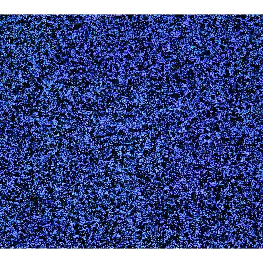
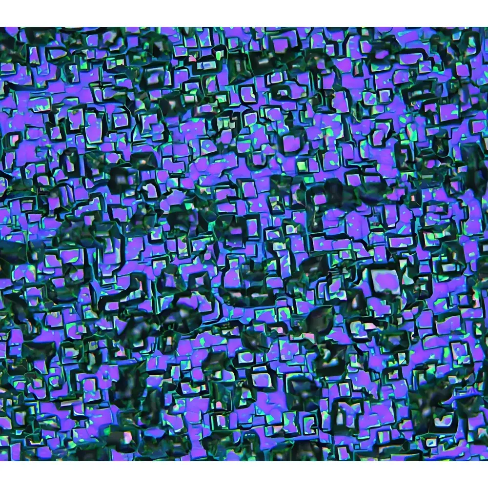
- Metallographic quality assurance: Grain size distribution analysis (ASTM E112), inclusion rating (ASTM E45), phase fraction measurement in heat-treated alloys, and weld microstructure evaluation.
- Failure analysis laboratories: Crack propagation path tracing, intermetallic compound (IMC) layer thickness measurement, and solder joint void analysis per IPC-J-STD-001.
- Academic and government research: Geological thin-section characterization, ceramic grain boundary mapping, and additive manufacturing powder morphology classification.
- Advanced packaging inspection: Underfill void detection, TSV (through-silicon via) sidewall roughness estimation, and fan-out wafer-level packaging (FOWLP) alignment verification.
FAQ
Does the LK-63R support DIC with all objective magnifications?
Yes—the 5×, 10×, 20×, 50×, and 100× semi-apochromatic objectives are specifically matched for DIC performance and include strain-free glass elements and precise shear alignment tolerances.
Can the system be upgraded to motorized Z-focus or automated stage control?
Yes—LEI-TECH offers factory-integrated motorized focus drives (with encoder feedback) and programmable XY stages compatible with the existing 6-inch platform interface and control bus.
Is the image analysis software compliant with regulatory audit requirements?
The optional ImagePro Metrology Suite includes full 21 CFR Part 11 compliance features: electronic signatures, immutable audit trails, user permission tiers, and data integrity validation logs.
What is the warranty coverage and service response time?
The LK-63R carries a standard 24-month parts-and-labor warranty; LEI-TECH maintains regional service centers across North America, EMEA, and APAC, with 7×24 remote diagnostics and on-site response within 3 business days under premium support contracts.
Are replacement objectives and accessories available through global distributors?
All UISC-corrected objectives, DIC prisms, polarizers, and stage adapters are stocked by authorized LEI-TECH distribution partners and ship with serialized calibration certificates traceable to NIST standards.


