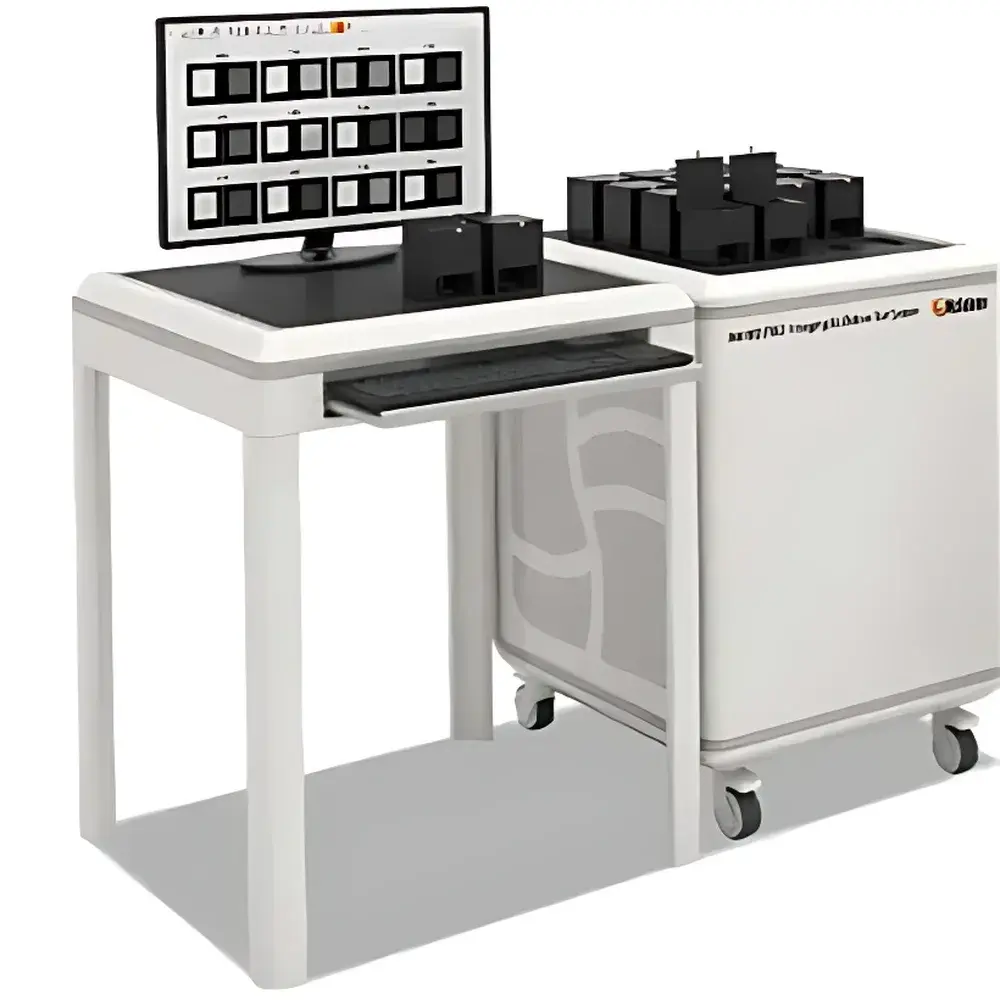
M6000 PIXX Imaging-Based Degradation Mechanism Analysis System for Perovskite QLED/OLED Devices
| Brand | McScience |
|---|---|
| Origin | South Korea |
| Model | M6000 PIXX |
| Device Type | Imaging-Based Electroluminescence Degradation Analyzer |
| Application Domain | Perovskite LED, OLED, QLED, Flexible Optoelectronic Devices, Inkjet-Printed Emissive Layer Development |
| Compliance Context | Designed for GLP-compliant lifetime testing workflows |
| Software Architecture | Windows-based acquisition and spatiotemporal EL intensity mapping platform |
Overview
The M6000 PIXX Imaging-Based Degradation Mechanism Analysis System is an engineered platform for high-resolution, time-resolved electroluminescence (EL) imaging and quantitative photophysical degradation tracking in emissive thin-film semiconductor devices. It operates on the principle of synchronized pixel-level current injection, voltage biasing, and low-noise scientific CMOS imaging under controlled environmental conditions (temperature, humidity, inert atmosphere optional). Unlike conventional integrated photometry or spot-measurement luminance decay systems, the M6000 PIXX captures full-field spatial heterogeneity—enabling direct correlation between local EL intensity decay kinetics, dark spot nucleation, current crowding zones, and interfacial delamination patterns. This capability is critical for elucidating root causes of non-uniform aging in perovskite light-emitting diodes (PeLEDs), quantum-dot LEDs (QLEDs), and multilayer organic light-emitting diodes (OLEDs), particularly those fabricated via solution-processing techniques such as inkjet printing.
Key Features
- High-sensitivity, back-illuminated sCMOS sensor with 4.2 MP resolution and sub-electron read noise, optimized for low-light EL imaging at operational drive currents (1–100 mA/cm²)
- Programmable multi-step stress protocols: constant-current, constant-voltage, pulsed-drive, and staircase-bias sequences with real-time feedback control
- Integrated environmental chamber (optional): temperature range −40 °C to +85 °C, humidity control 5–95% RH non-condensing, N₂ purge port for oxygen/moisture-sensitive perovskite studies
- Automated stage with 100 mm × 100 mm travel, 0.5 µm repeatability, enabling precise registration across repeated imaging sessions over weeks-long lifetime tests
- Multi-channel synchronization: hardware-triggered coordination between source measure unit (SMU), image acquisition, and environmental sensors (T/RH) at microsecond-level timing precision
- Modular optical path: interchangeable objectives (2.5× to 20×), bandpass filters (365–1050 nm), and optional NIR-enhanced detection for QD and deep-red PeLED characterization
Sample Compatibility & Compliance
The M6000 PIXX supports substrates up to 150 mm × 150 mm, including glass, PET, PI, and stainless-steel foils—compatible with rigid, flexible, and stretchable device architectures. Electrode configurations include ITO/PEDOT:PSS/EmLayer/Ca/Al, NiOₓ/perovskite/TPBi/LiF/Al, and inverted QD structures. All electrical interfaces comply with IEEE 488.2 (GPIB) and USB 3.2 Gen 1 standards for interoperability with third-party SMUs and environmental controllers. The system architecture aligns with Good Laboratory Practice (GLP) documentation requirements: audit-trail-enabled software logs all parameter changes, timestamps, user IDs, and raw image metadata (EXIF-compliant). While not certified as FDA 21 CFR Part 11 compliant out-of-the-box, the platform supports configuration-controlled validation packages for regulated R&D environments requiring electronic record integrity.
Software & Data Management
Acquisition and analysis are executed via PIXXControl v4.x, a Windows 10/11-native application built on Qt and Python 3.9 core libraries. The software provides real-time pixel-wise EL intensity normalization (relative to initial frame), temporal decay curve fitting (bi-exponential, stretched exponential models), and spatial variance mapping (coefficient of variation overlays). Export formats include TIFF (16-bit linear), HDF5 (for large time-series stacks), CSV (ROI-integrated metrics), and JSON (metadata-rich protocol definitions). Batch processing pipelines support automated dark-frame subtraction, flat-field correction, and drift compensation using fiducial markers. Data provenance is preserved through embedded hash signatures and version-stamped project archives—facilitating reproducibility in peer-reviewed publications and internal technology transfer reports.
Applications
- Quantifying localized degradation onset in inkjet-printed PeLED arrays—correlating nozzle-to-nozzle variability with EL quenching kinetics
- Mapping interfacial ion migration pathways in layered perovskite emitters via time-lapse EL heterogeneity evolution under reverse-bias stress
- Evaluating encapsulation efficacy by monitoring edge-invasion dynamics of moisture-induced dark spot propagation
- Validating charge-transport layer stability (e.g., NiOₓ, ZnO, TFB) through spatially resolved turn-on voltage shift analysis
- Supporting accelerated lifetime modeling (IEC 62717 Annex D) by generating Arrhenius-plot-ready datasets across multiple stress temperatures
- Enabling failure mode identification for display-grade RGB QLED microdisplays under pulse-width-modulated driving schemes
FAQ
What types of emissive layers can be characterized with the M6000 PIXX?
Perovskite nanocrystals (CsPbBr₃, FAPbBr₃), colloidal quantum dots (CdSe/ZnS, InP/ZnS), small-molecule and polymer OLED hosts (e.g., CBP, PVK, TFB), and thermally activated delayed fluorescence (TADF) emitters.
Does the system support in situ electrical impedance spectroscopy (EIS)?
No—EIS requires separate potentiostat integration; however, the M6000 PIXX provides synchronized DC/AC bias triggering to external impedance analyzers via TTL output ports.
Can raw image data be exported for custom MATLAB or Python analysis?
Yes—TIFF and HDF5 exports retain full bit-depth, metadata, and spatial calibration information; Python API wrappers are available under NDA for advanced algorithm development.
Is remote operation supported for long-term unattended testing?
Yes—Windows Remote Desktop-compatible architecture with watchdog timer, automatic error logging, and SMTP alerting upon protocol interruption or environmental excursion.
What is the minimum detectable luminance change per pixel during lifetime tracking?
Under standard 10 ms exposure at 25 °C, the system resolves ΔL/L₀ ≥ 0.3% with <5% coefficient of variation across uniform test areas (measured using calibrated reference OLED tiles).


