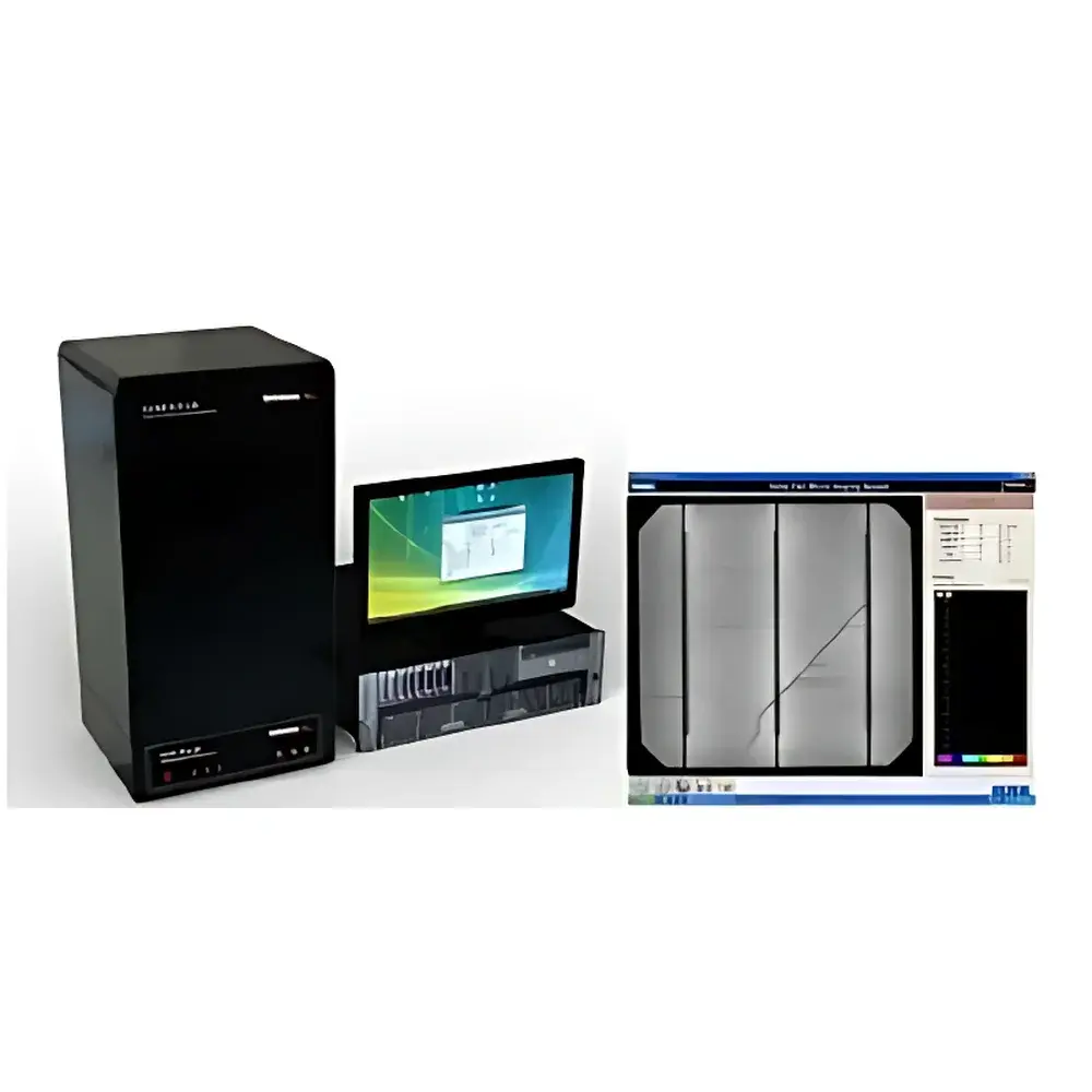

McScience LAB Desktop Multifunctional Electroluminescence (EL) Defect Inspection System for Solar Cells
| Brand | McScience |
|---|---|
| Origin | Imported |
| Model | LAB |
| Power Supply | DC/Pulse |
| Operation Modes | Constant Current / Constant Voltage |
| Voltage Range | -20 V to +5 V |
| Current Options | 30 mA / 1 A / 20 A (user-selectable) |
| Imaging Sensor | High-Resolution CCD |
| Sample Compatibility | Individual Solar Cells & Large-Area PV Modules |
| Additional Capabilities | Integrated PL Imaging Option, Reflectance Mapping, LBIC (Light Beam Induced Current), Visual Inspection |
Overview
The McScience LAB Desktop Multifunctional Electroluminescence (EL) Defect Inspection System is an engineered solution for non-destructive, high-sensitivity characterization of crystalline silicon (c-Si), thin-film, and emerging photovoltaic devices. Operating on the principle of electroluminescence—where a forward-biased solar cell emits near-infrared (NIR) photons proportional to local minority carrier recombination—the system captures spatially resolved luminescence intensity maps with sub-millimeter resolution. Unlike thermal imaging or visual inspection alone, EL imaging directly correlates with electrical performance degradation mechanisms, enabling root-cause analysis of defects affecting fill factor, open-circuit voltage, and series resistance distribution. Designed for both R&D laboratories and pilot-line process validation, the LAB platform supports flexible configuration—including optional integration with photoluminescence (PL) imaging—to differentiate between bulk lifetime-limited regions and contact-related losses. Its modular architecture accommodates varying throughput requirements without compromising measurement fidelity or repeatability.
Key Features
- Programmable DC/pulsed current/voltage excitation source with precision control over bias conditions, supporting both forward and reverse polarity EL acquisition for junction integrity assessment.
- High-sensitivity, cooled CCD imaging sensor optimized for 900–1200 nm spectral response, delivering low-noise, high-dynamic-range EL images under ambient or darkroom conditions.
- Multi-range current sourcing capability (30 mA, 1 A, or 20 A) enables consistent excitation across diverse cell architectures—from lab-scale perovskite mini-modules to industrial-size 210 mm mono-Si wafers.
- Modular hardware interface supports seamless integration of optional modules: PL imaging head, reflectance mapping stage, LBIC scanning unit, and macro/micro visual inspection optics.
- Standardized mechanical stage with XYZ adjustment and tilt compensation ensures repeatable positioning for comparative time-series analysis and cross-lot qualification.
- Fully configurable software interface compliant with ASTM E2848-22 (Standard Practice for Reporting Photovoltaic Non-Destructive Evaluation Data) metadata conventions.
Sample Compatibility & Compliance
The LAB system accommodates standard test coupons (e.g., 156 × 156 mm², 166 × 166 mm², 182 × 182 mm², 210 × 210 mm² c-Si cells), half-cut and shingled configurations, as well as laminated full-size modules up to 2.4 m × 1.3 m using optional motorized gantry extension. All optical and electrical interfaces comply with IEC 61215-2 MQT 07 (Electroluminescence Imaging) and IEC 62788-5-2 (Measurement of Series Resistance Distribution). Data acquisition workflows support GLP-compliant audit trails, including operator ID, timestamped parameter logs, image hash verification, and version-controlled calibration records—fully traceable for ISO/IEC 17025-accredited labs.
Software & Data Management
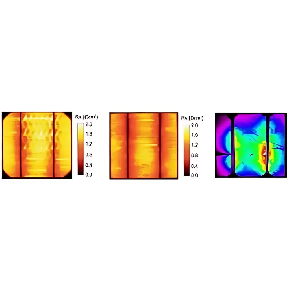
The proprietary McScience EL Studio software provides integrated acquisition, processing, and reporting functionality. It includes automated defect classification algorithms trained on >10,000 annotated EL images (micro-cracks, finger interruptions, solder bond voids, edge delamination, hotspots), with user-definable thresholds for intensity deviation, gradient discontinuity, and morphological signature matching. Raw TIFF and HDF5 data exports are compatible with MATLAB, Python (OpenCV, scikit-image), and commercial statistical process control (SPC) platforms. Audit-ready reports include summary statistics (mean intensity, std dev, defect density/mm²), annotated overlays, and comparative side-by-side module analysis—all exportable in PDF/A-2b or CSV formats. Software validation documentation is available upon request for FDA 21 CFR Part 11 compliance readiness.
Applications
- R&D process development: Quantifying impact of screen-printing paste formulation, firing profile optimization, and passivation layer uniformity on local recombination activity.
- Production line QA/QC: Rapid screening of incoming wafers, post-cell fabrication, and final module assembly for latent structural or interfacial defects.
- Fault analysis in field-degraded modules: Correlating EL signatures (e.g., localized dark areas, gridline discontinuities) with IV curve anomalies and thermal imaging results.
- Advanced characterization: Combined EL/PL mapping to decouple bulk lifetime from surface recombination velocity; reflectance mapping for anti-reflection coating homogeneity assessment.
- Standards laboratory use: Reference-grade EL imaging for inter-laboratory round-robin studies aligned with IEA-PVPS Task 13 protocols.
FAQ
What types of solar cell technologies can the LAB system inspect?
The system is validated for monocrystalline and multicrystalline silicon, CIGS, CdTe, and perovskite-based devices. Support for tandem structures requires optional NIR-enhanced optics.
Is the system compatible with existing cleanroom infrastructure?
Yes—it operates at standard atmospheric pressure and ambient temperature, with ESD-safe chassis design and Class 1 laser safety certification for optional PL integration.
Can EL data be correlated with electrical measurements such as IV or Suns-Voc?
Yes—synchronized triggering allows concurrent acquisition of EL images and point-contact IV traces; exported datasets include time-aligned metadata for cross-modal regression analysis.
Does the software support automated pass/fail grading against internal specifications?
Yes—custom rule engines allow defining multi-parameter acceptance criteria (e.g., max crack length per cm², minimum relative intensity at busbars) with configurable alarm thresholds and SPC charting.
What service and calibration options are available?
Annual NIST-traceable radiometric calibration, on-site preventive maintenance, remote diagnostics, and application-specific training packages are offered globally through McScience’s authorized service network.


