Mica Sheets (V1/V2 Grade) – Hefei Kejing High-Purity Natural Mica Substrates for Electron Microscopy and AFM
| Brand | Hefei Kejing |
|---|---|
| Origin | Anhui, China |
| Grade Classification | V1 (Ultra-Thin) / V2 (Standard Thickness) |
| Thickness Tolerance | ±0.01 mm |
| Surface Roughness (Rq) | <0.3 nm (V1), <0.5 nm (V2) |
| Optical Transparency | >92% (400–800 nm) |
| Packaging | Class 1000 Cleanroom-Processed, Sealed in Class 100 Cleanroom Bags |
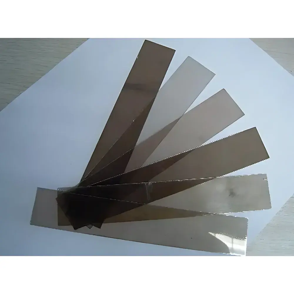
| Standard Dimensions | V1 — Ø9.9 mm × 0.21 mm, Ø20 mm × 0.21 mm, 15 × 15 mm × 0.15–0.177 mm |
Overview
Hefei Kejing’s high-purity natural mica sheets are precision-cleaved substrates engineered for demanding surface science applications requiring atomic-level flatness, chemical inertness, and exceptional dielectric stability. Sourced from select muscovite deposits and processed under controlled cleanroom conditions, these mica substrates serve as foundational platforms for high-resolution imaging and nanoscale characterization. Unlike synthetic alternatives, natural mica offers intrinsic crystalline order with minimal lattice defects, enabling reliable charge dissipation and stable sample anchoring during scanning probe microscopy (SPM), transmission electron microscopy (TEM) grid preparation, and thin-film deposition studies. The V1 grade delivers ultra-thin mechanical cleavage (0.15–0.21 mm thickness) optimized for electron transparency and minimal substrate interference in low-energy electron beam applications; the V2 grade provides enhanced mechanical rigidity (0.27 mm) while retaining sub-nanometer surface uniformity—ideal for repeated tip-based manipulation and long-duration cell adhesion assays.
Key Features
- Natural muscovite composition with verified stoichiometric consistency (KAl2(AlSi3O10)(OH)2) and negligible Fe/Mg impurities (<50 ppm by ICP-MS)
- Controlled mechanical exfoliation yielding atomically smooth basal planes—surface roughness quantified via AFM: Rq < 0.3 nm (V1), Rq < 0.5 nm (V2) over 10 × 10 µm scan areas
- Optical clarity across visible to near-UV spectrum (400–800 nm), enabling simultaneous optical correlation with electron or force microscopy
- Thermal stability up to 600 °C in inert atmosphere; compatible with standard plasma cleaning (O2/Ar), UV-ozone, and mild solvent rinsing protocols
- Batch-certified dimensional tolerance: ±0.05 mm in lateral dimensions, ±0.01 mm in thickness—traceable to NIST-traceable micrometry
- Class 1000 cleanroom processing with final packaging in ISO Class 5 (100) cleanroom bags, certified per ISO 14644-1
Sample Compatibility & Compliance
These mica substrates are routinely validated for use in GLP-compliant laboratories conducting nanomaterial characterization, biomembrane reconstitution, and 2D crystallography. Their surface chemistry supports reproducible electrostatic adsorption of negatively charged biomolecules (e.g., DNA, phospholipid vesicles, amyloid fibrils) without covalent modification. All batches undergo spectral verification via FTIR (absence of hydrocarbon contamination bands at 2850–2960 cm−1) and XRD (sharp (002) peak at 2θ = 8.8°, FWHM < 0.15°). Documentation includes material traceability reports, cleanroom processing logs, and surface contamination assay summaries—fully aligned with ASTM E2500-21 (Good Practice for Specification of Pharmaceutical and Biotechnology Equipment) and ISO/IEC 17025:2017 requirements for reference material providers.
Software & Data Management
While mica sheets themselves are passive substrates, their integration into automated workflows is supported through compatibility with industry-standard instrument control platforms—including Bruker NanoScope Analysis, Thermo Fisher Velox, and JEOL EMIP software suites. Batch-specific lot numbers are laser-etched on packaging labels and linked to digital certificates of analysis (CoA) accessible via secure portal login. CoAs include AFM topography thumbnails, spectral validation charts, and particulate count data per ISO 14644-1 Annex B. Audit trails for cleanroom handling and packaging events comply with FDA 21 CFR Part 11 electronic record requirements when accessed through authenticated institutional accounts.
Applications
- Atomic force microscopy (AFM) substrate for single-molecule force spectroscopy and time-lapse membrane dynamics
- Electron-transparent support film base for cryo-TEM grid fabrication (e.g., graphene/mica hybrid substrates)
- Template for epitaxial growth of 2D materials (MoS2, h-BN) and van der Waals heterostructures
- In situ electrochemical AFM (EC-AFM) cell windows due to high dielectric strength (>118 MV/m) and low leakage current (<1 pA at 10 V)
- Cell culture platform for high-resolution live-cell imaging—enabling correlated fluorescence, SEM, and AFM of adherent mammalian cells
- Calibration reference for step-height metrology in profilometry and interferometry systems
FAQ
What cleavage plane is used for these mica sheets?
All sheets are cleaved along the (001) basal plane, ensuring maximal surface periodicity and minimizing step edges. Cleavage is performed mechanically under nitrogen-purged laminar flow to prevent hydration-induced surface reconstruction.
Can V1-grade mica be used in high-vacuum TEM stages?
Yes—V1 sheets meet outgassing specifications per ASTM E595 for total mass loss (TML < 0.5%) and collected volatile condensable materials (CVCM < 0.05%) after 24 h at 125 °C under 5×10⁻⁶ Torr.
Is hydrophilic treatment available?
Standard sheets are native-hydrophilic (contact angle ~25°); argon plasma activation (50 W, 60 s) reduces contact angle to 72 mN/m—protocol documented in CoA appendix.
How are thickness tolerances verified?
Each lot undergoes non-contact optical interferometry (Zygo NewView 9000) with calibrated 5× Mirau objective; 20 random points per sheet are measured and statistically reported in the CoA.
Do you provide custom cutting or metallization?
Custom geometries (e.g., rectangular slits, fiducial markers) and e-beam evaporation of Cr/Au (5/30 nm) or Ti/Pt (5/20 nm) layers are available under NDA—lead time: 10–14 business days post-approval.


