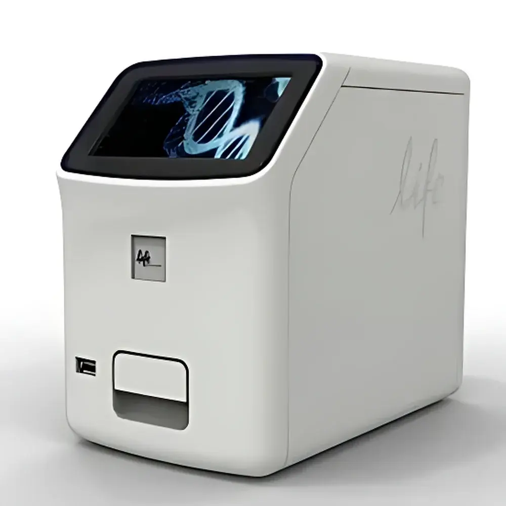
MicronX X-Ray Fluorescence Thickness Analyzer
| Origin | USA |
|---|---|
| Manufacturer Type | Authorized Distributor |
| Origin Category | Imported |
| Model | MicronX |
| Pricing | Available Upon Request |
Overview
The MicronX X-Ray Fluorescence (XRF) Thickness Analyzer is a benchtop micro-spot elemental thickness measurement system engineered for high-precision, non-destructive analysis of thin films and multi-layer coatings in semiconductor fabrication, advanced packaging, PCB manufacturing, and precision electroplating applications. It operates on the fundamental principle of energy-dispersive X-ray fluorescence: a focused X-ray beam excites characteristic secondary X-rays from atoms within the sample; the intensity and energy of emitted fluorescence photons are quantitatively correlated to elemental composition and layer thickness via fundamental parameter (FP) algorithms and empirical calibration models. Unlike destructive cross-sectioning or stylus profilometry, the MicronX delivers rapid, repeatable measurements without physical contact or sample preparation—critical for process control in cleanroom environments where wafer integrity and yield assurance are paramount.
Key Features
- Micron-Scale Spot Analysis: Equipped with a high-brightness micro-focus X-ray tube and polycapillary optics, the MicronX achieves a minimum analysis spot size of 50 µm—enabling precise targeting of fine-pitch features such as bump under-bump metallization (UBM), redistribution layers (RDL), and solder mask openings.
- Multi-Layer Capability: Supports quantitative thickness determination of up to seven discrete layers in a single measurement sequence—including complex stacks like Ti/Cu/Ni/Au on silicon wafers or Sn/Ag/Cu over NiP on leadframes—using iterative FP modeling validated against certified reference materials (CRMs).
- High-Resolution Imaging & Navigation: Integrated 10-megapixel CCD camera with motorized zoom provides real-time optical imaging up to 300× digital magnification; combined with motorized XYZ stage (±0.5 µm repeatability), users can rapidly locate features, define measurement grids, and correlate spectral data with visual morphology.
- Automated Mapping & Distribution Analysis: Precision motorized stage enables programmable raster scanning across user-defined areas (up to 100 × 100 mm). Element-specific thickness maps (e.g., Cu thickness uniformity across a 300-mm wafer quadrant) are generated with pixel resolution down to 5 µm, supporting statistical process control (SPC) and defect root-cause analysis.
- Robust Hardware Architecture: Sealed vacuum chamber optional for light-element sensitivity (e.g., Al, Si, P); helium purge mode available for enhanced detection of Na–Cl in organic dielectrics. All electronics conform to IEC 61000-4 EMC standards; radiation shielding meets ANSI N43.3 Class I safety requirements.
Sample Compatibility & Compliance
The MicronX accommodates flat, rigid substrates up to 300 mm in diameter and 50 mm in thickness—including silicon wafers, ceramic substrates, FR-4 PCBs, and metal leadframes. Sample height variation is compensated by auto-focus laser triangulation. Measurement accuracy is traceable to NIST-traceable thin-film standards (e.g., NIST SRM 2136, 2137), and system performance verification follows ASTM E1598–22 (“Standard Practice for Calibration of XRF Coating Thickness Instruments”). The instrument supports GLP/GMP-compliant operation through configurable user access levels, electronic signatures, and full audit trail logging per FDA 21 CFR Part 11 requirements when paired with optional compliant software modules.
Software & Data Management
Controlled via Windows-based MicronX Studio software, the system provides intuitive workflow-driven interfaces for method development, measurement execution, and reporting. Each measurement session records full spectral metadata—including tube voltage/current, live time, dead time, detector temperature, and stage coordinates—ensuring full analytical traceability. Batch processing supports ISO/IEC 17025-aligned uncertainty estimation using Monte Carlo propagation. Export formats include CSV, XML, PDF reports (with embedded spectra and maps), and direct integration with MES/SPC platforms via OPC UA or SQL database connectors. Raw spectral data (.spe) and processed results (.xrf) are stored in vendor-neutral formats for third-party reanalysis.
Applications
- Thickness and composition verification of sputtered, evaporated, or electroplated metal stacks (e.g., TiN/Ti/Cu in BEOL interconnects)
- Quality control of solder paste deposits and reflowed solder bumps in flip-chip and 2.5D/3D packaging
- Measurement of barrier layers (e.g., TaN, CoWP) and seed layers in advanced node copper dual-damascene processes
- Quantitative analysis of NiAu, NiPdAu, or ENIG surface finishes on PCBs and connectors
- Failure analysis of delamination or interdiffusion in multi-layer metallizations via depth-profiling mode
FAQ
What is the minimum detectable thickness for gold on nickel using the MicronX?
Typical detection limit is ~0.3 nm for Au on Ni under optimized conditions (50 kV, 1 µA, 100 s live time), dependent on matrix absorption and spectral overlap.
Can the MicronX measure organic layers such as photoresist or polyimide?
Yes—via light-element optimized configurations (He purge or vacuum), it quantifies C, N, O, and F in polymer films; thickness accuracy depends on density homogeneity and substrate contrast.
Is spectral deconvolution automated for overlapping peaks (e.g., Cr Kβ and Fe Kα)?
Yes—MicronX Studio employs least-squares fitting with physically constrained background modeling and peak shape libraries derived from reference spectra.
Does the system support automated pass/fail judgment based on tolerance limits?
Yes—user-defined specification limits trigger color-coded visual alerts and exportable SPC charts (X-bar/R, Cp/Cpk) directly from measurement batches.
How is calibration maintained over time?
Daily system checks use built-in reference foils; quarterly recalibration is recommended using NIST-traceable multilayer standards; drift correction algorithms compensate for detector aging and tube output fluctuations.


")