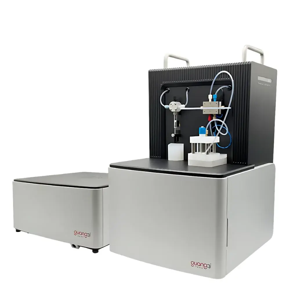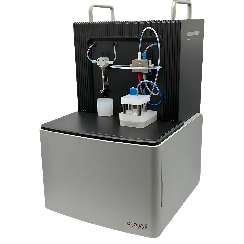
Microtech ulaser/ilaser Desktop Maskless Laser Direct-Write Lithography System
| Brand | MICROTECH |
|---|---|
| Model | ulaser/ilaser |
| Minimum Feature Size | 2 µm |
| Laser Spot Diameter | 1 µm |
| Acceleration Voltage | 30 kV |
| Origin | Imported |
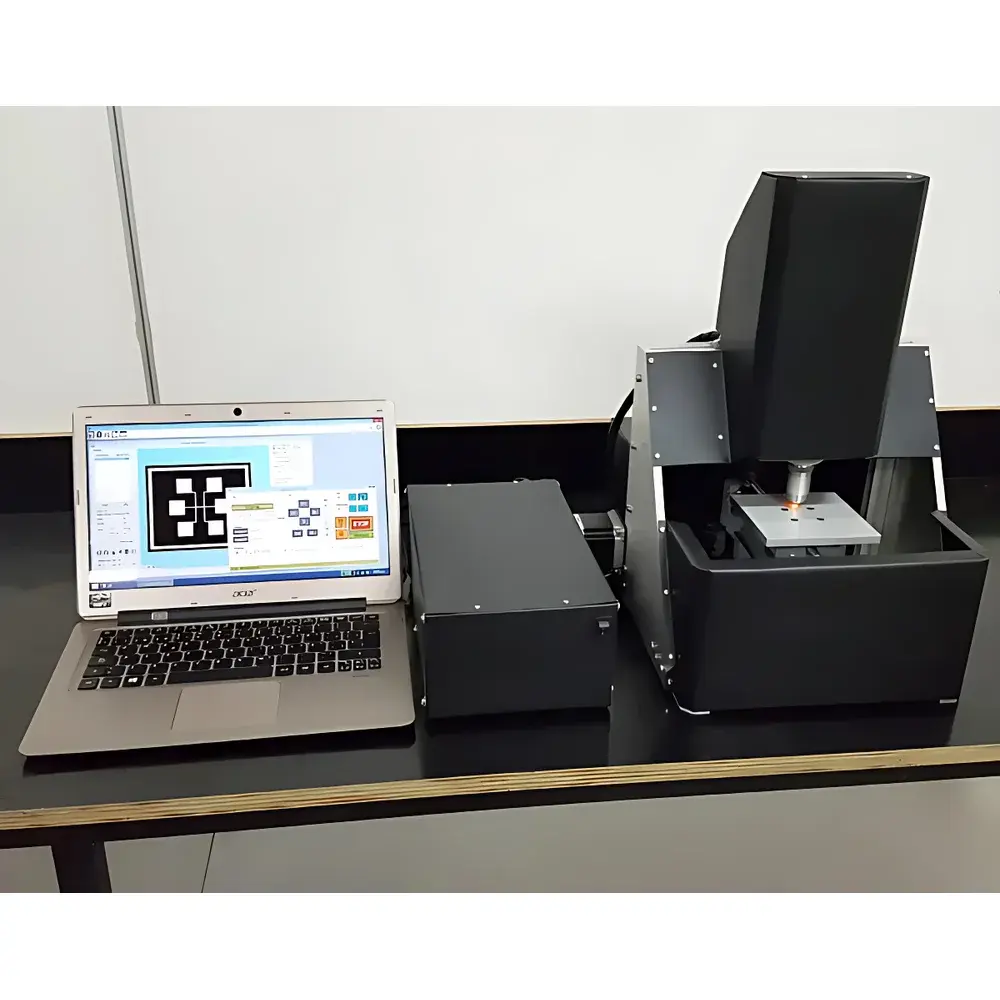
| Configuration | Integrated desktop platform with fully automated control |
| Compliance | Designed for R&D and pilot-line semiconductor fabrication environments |
Overview
The Microtech ulaser/ilaser Desktop Maskless Laser Direct-Write Lithography System is an engineered solution for rapid prototyping and low-to-medium volume nanofabrication in academic laboratories, microelectronics R&D centers, and advanced packaging development facilities. Unlike conventional photolithography—which relies on costly, time-intensive photomasks—the ulaser/ilaser system employs a focused laser beam (not electron beam, despite common misclassification in marketing materials) scanned across a photosensitive resist layer under high-precision galvanometric or piezoelectric positioning control. This maskless approach enables immediate pattern transfer from CAD layout files without intermediate mask fabrication, significantly shortening design-to-fabrication cycles. The system operates at a nominal acceleration voltage of 30 kV to drive the laser excitation source—consistent with solid-state UV or deep-UV laser diodes integrated into a compact optical path—and achieves a minimum resolvable feature size of 2 µm with a diffraction-limited spot diameter of 1 µm. Its desktop footprint and integrated vacuum-free optical train eliminate cleanroom dependency for initial process validation, while maintaining alignment stability and thermal drift compensation suitable for sub-5 µm registration accuracy over write fields up to 100 mm × 100 mm.
Key Features
- Fully automated desktop platform with integrated motion control, real-time focus tracking, and auto-calibration routines for beam alignment and stage flatness compensation
- High-resolution laser scanning optics delivering ≤1 µm spot size and ≤2 µm minimum line width in standard positive-tone photoresists (e.g., AZ® series, ma-N, SU-8)
- Large write field capability (up to 100 mm × 100 mm per exposure) supported by stitched-field overlay with <±150 nm inter-field registration repeatability
- Open-format GDSII and OASIS file import with built-in polygon fracturing, proximity effect correction (PEC), and dose modulation algorithms
- Modular resist compatibility: optimized for UV-curable, e-beam resists, and hybrid organic-inorganic precursors used in MEMS, photonics, and flexible electronics patterning
- Embedded environmental monitoring (temperature, humidity, vibration) with logging for GLP-compliant process documentation
Sample Compatibility & Compliance
The ulaser/ilaser system supports substrates up to 150 mm in diameter and 10 mm thick—including silicon wafers, fused silica, glass, polymer films (PI, PET), and metal-coated foils. It accommodates both spin-coated and spray-deposited resist layers ranging from 100 nm to 5 µm thickness. Process parameters are configurable to meet ASTM F2782 (Standard Practice for Electron Beam and Laser Beam Lithography Pattern Transfer) and ISO/IEC 17025 calibration traceability requirements when paired with certified reference standards. While not classified as a production-grade tool per SEMI S2/S8 safety certification, its operational envelope complies with IEC 60825-1:2014 (laser product safety) and EU Machinery Directive 2006/42/EC. For regulated environments, audit trails, user access levels, and electronic signatures can be enabled to align with FDA 21 CFR Part 11 expectations during qualification.
Software & Data Management
Control and pattern generation are managed via Microtech’s proprietary LithoSuite™ software—a Windows-based application supporting offline job preparation, multi-layer alignment scripting, and real-time dosimetry feedback. All exposure logs, stage position traces, and environmental sensor data are stored in SQLite databases with SHA-256 hash integrity verification. Export formats include CSV, TIFF stack (for dose map visualization), and standardized metrology-ready .STL or .STEP exports for cross-platform CAD integration. Optional API modules enable Python-driven automation (via RESTful endpoints) and integration into MES platforms such as Siemens Opcenter or Camstar for traceable lot-level execution.
Applications
- Rapid iteration of photonic integrated circuit (PIC) layouts, including grating couplers, waveguide bends, and micro-ring resonators
- Prototyping of microfluidic channel networks with sub-10 µm wall definition for organ-on-chip and lab-on-chip devices
- Direct-write fabrication of diffractive optical elements (DOEs), microlens arrays, and anti-reflective surface textures
- Maskless patterning of transparent conductive oxides (ITO, AZO) for touch sensor electrodes and flexible display interconnects
- Research-scale fabrication of plasmonic nanostructures and metamaterial unit cells requiring local periodicity control
- Education and training in nanofabrication principles—offering hands-on exposure to lithographic resolution limits, proximity effects, and process window analysis
FAQ
Is this system based on electron beam or laser technology?
It is a laser direct-write system utilizing a focused ultraviolet or deep-UV laser source—not an electron beam column. The “30 kV” specification refers to the excitation voltage driving the solid-state laser diode module, not beam acceleration.
What resist types are validated for use with this platform?
AZ® 1518, ma-N 2401, SU-8 2000 series, and PMMA A4 are routinely qualified. Custom resist formulations may require dose calibration using the included reference test patterns.
Can the system perform multi-layer alignment?
Yes—using fiducial-based optical recognition and motorized Z-stage autofocus, overlay accuracy of ±200 nm (3σ) is achievable between layers when using standard alignment marks.
Does it support grayscale lithography?
Grayscale exposure is supported through variable dwell-time modulation and programmable intensity profiling, enabling topography-defined structures such as Fresnel lenses and micro-optical surfaces.
What maintenance is required for long-term stability?
Annual recalibration of galvo scanners and optical power metering is recommended. No consumables beyond standard cleanroom wipes and nitrogen purge gas (optional) are required.