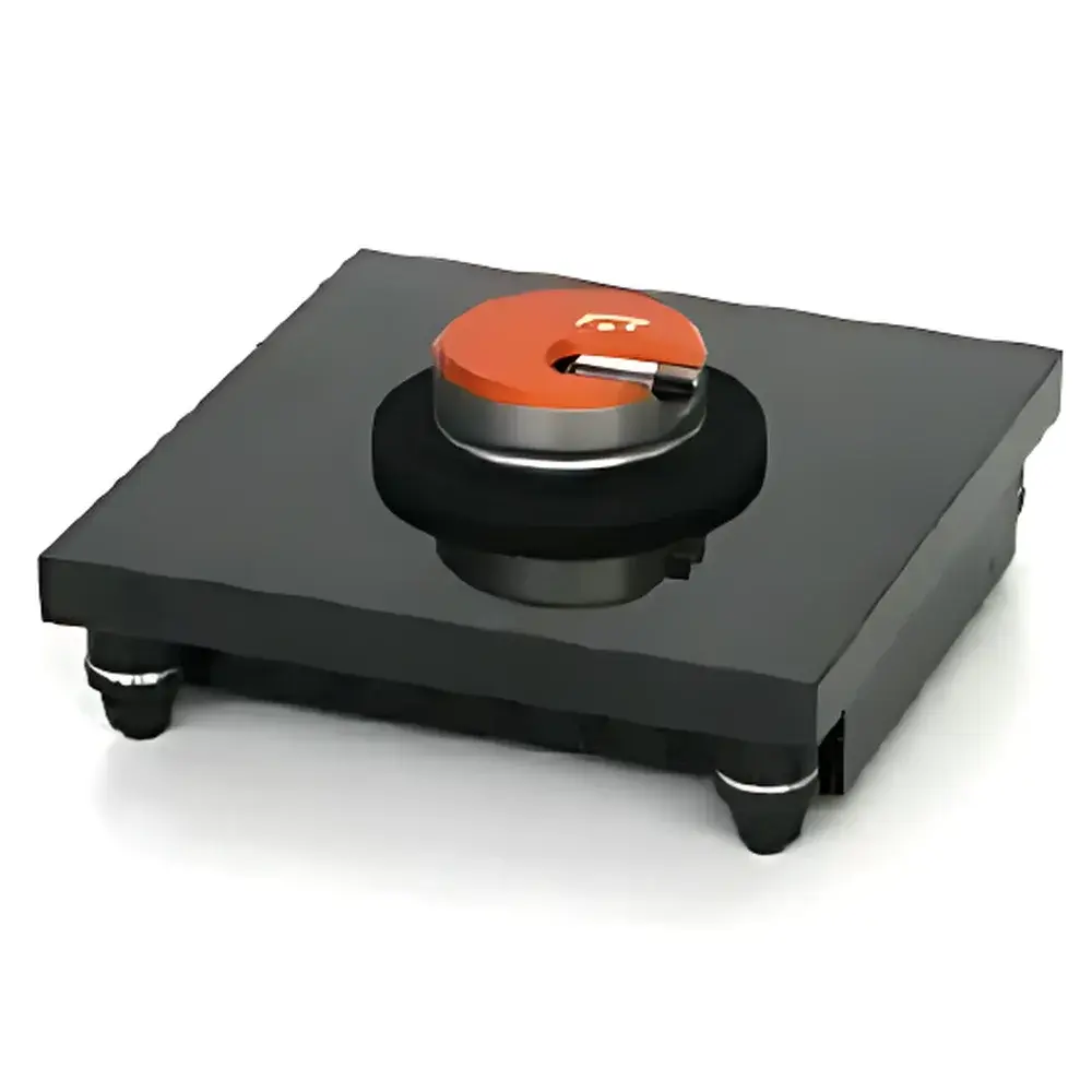
Nanosurf Naio STM Scanning Tunneling Microscope
| Brand | Nanosurf |
|---|---|
| Origin | Switzerland |
| Model | Naio STM |
| Position Detection Noise | 0.15 nm |
| Sample Area | 500 nm × 500 nm |
| XY Scan Range | 500 nm × 500 nm |
| XY Resolution | 7.6 pm |
| Z Scan Range | 200 nm |
| Z Resolution | 3 pm |
| Maximum Tunneling Current | 100 nA |
| Sample Stage Diameter | 10 mm |
| Max Sample Thickness | 3 mm |
| Imaging Modes | Constant-Current & Constant-Height |
| Spectroscopy Modes | I–V, I–z |
| Max Image Pixels | 2048 × 2048 |
| Max Spectral Points | 32768 |
| XY Tilt Compensation | Hardware-based |
| Interface | USB 2.0 |
| Dimensions | 204 mm × 204 mm × 104 mm |
| Weight | 3.45 kg |
Overview
The Nanosurf Naio STM is a compact, fully integrated scanning tunneling microscope engineered for high-resolution surface characterization at the atomic scale. Operating on the quantum mechanical principle of electron tunneling, the Naio STM measures minute variations in tunneling current between a conductive tip and a conductive sample surface under ultra-stable conditions. Its monolithic design integrates the controller, scanner, sample stage, and passive vibration isolation into a single benchtop unit—eliminating complex external cabling, alignment procedures, and environmental sensitivity typically associated with conventional STM systems. Designed and manufactured in Switzerland, the instrument delivers sub-picometer spatial resolution (7.6 pm XY, 3 pm Z) and exceptional thermal and mechanical stability, enabling reliable imaging and spectroscopy in standard laboratory environments—without requiring dedicated cleanrooms or active acoustic enclosures.
Key Features
- Monolithic architecture with integrated electronics, piezoelectric scanner, and passive vibration isolation—no external rack-mounted controllers or separate preamplifiers required.
- Ultra-low position detection noise of 0.15 nm RMS enables stable atomic-scale imaging on HOPG, Au(111), and other well-ordered conductive surfaces.
- High-precision XY scan range of 500 nm × 500 nm with 7.6 pm step resolution and hardware-based XY tilt compensation for accurate topographic reconstruction on mildly inclined samples.
- Z-axis extension of 200 nm with 3 pm resolution and motorized approach mechanism for repeatable, non-contact tip-sample engagement.
- Compact footprint (204 × 204 × 104 mm) and lightweight construction (3.45 kg) facilitate rapid deployment across shared labs, teaching facilities, or portable field applications.
- USB 2.0 interface ensures plug-and-play compatibility with Windows, macOS, and Linux platforms; no proprietary drivers or dongles required.
Sample Compatibility & Compliance
The Naio STM is optimized for conductive and semi-conductive samples up to 10 mm in diameter and 3 mm in thickness. Standard reference materials—including highly oriented pyrolytic graphite (HOPG) and atomically flat gold substrates—are included for calibration and performance verification. The system supports both constant-current and constant-height imaging modes, accommodating diverse surface electronic properties and topographies. All hardware and firmware comply with CE marking requirements for electromagnetic compatibility (EMC Directive 2014/30/EU) and low-voltage safety (LVD Directive 2014/35/EU). While STM itself does not fall under FDA or ISO 13485 regulatory scopes, its data acquisition architecture supports audit-ready operation: raw data files are timestamped, unalterable, and stored in open HDF5 format—enabling traceability per GLP and internal QA protocols.
Software & Data Management
Acquisition and analysis are performed using Nanosurf’s proprietary WSxM-compatible software suite, distributed on optical media and available as digital download. The software provides real-time feedback control, multi-channel simultaneous recording (topography, current, Z-piezo voltage), and post-processing tools including FFT filtering, line profile extraction, grain analysis, and automated step-height quantification. Spectroscopic capabilities include point-spectroscopy (I–V and I–z curves) with up to 32,768 sampling points per curve, and grid-based spectroscopy across user-defined regions. All measurement parameters—including setpoint, gain, integral time, and filter settings—are saved with each dataset. Export options include ASCII, PNG, TIFF, and HDF5 formats, ensuring interoperability with MATLAB, Python (via h5py), and third-party statistical packages. No cloud dependency or subscription licensing is required.
Applications
- Atomic-resolution imaging of graphene, transition metal dichalcogenides (TMDs), and surface reconstructions on Si(111) or Cu(110).
- In situ electrochemical STM studies on electrode interfaces under potentiostatic control (when coupled with compatible potentiostats).
- Nanoscale defect identification and electronic state mapping via dI/dV spectroscopy on superconductors and topological insulators.
- Teaching laboratories: hands-on instruction in quantum tunneling, piezoelectric actuation, feedback control theory, and surface science fundamentals.
- Quality assurance of thin-film deposition processes where surface roughness, grain size, and domain boundaries impact device performance.
FAQ
Is the Naio STM capable of ultra-high vacuum (UHV) operation?
No—the Naio STM is designed for ambient or inert-gas environments only. It is not UHV-compatible due to its integrated passive isolation base and non-bakeable mechanical construction.
Can non-conductive samples be imaged?
Not directly. STM requires finite electronic density of states at the Fermi level. Insulating samples must be coated with an ultrathin conductive layer (e.g., carbon or Cr/Au) or studied using complementary techniques such as AFM.
What is the typical tip lifetime under standard operating conditions?
With proper handling and routine cleaning (e.g., field ion microscopy conditioning), tungsten or Pt/Ir tips typically sustain >50 hours of continuous imaging on atomically flat HOPG before noticeable degradation in resolution or signal-to-noise ratio.
Does the system support external trigger synchronization?
Yes—digital I/O ports allow TTL-level synchronization with external equipment such as lasers, pulse generators, or lock-in amplifiers for time-resolved or pump-probe measurements.
Is technical support and firmware updates provided after purchase?
Yes—Nanosurf offers complimentary firmware updates and remote diagnostic support for the duration of the standard 2-year warranty period, extendable upon request.


