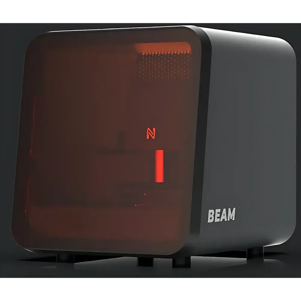
NILT BEAM Desktop Direct Laser Writing System
| Brand | NILT |
|---|---|
| Origin | Denmark |
| Manufacturer Type | Authorized Distributor |
| Origin Category | Imported |
| Model | BEAM |
| Exposure Mode | Proximity-style Direct Write |
| Resolution | ≤500 nm (line width) |
| Light Source | UV Diode Lasers |
| Wavelengths | 365 nm, 385 nm, 405 nm |
| Illumination Uniformity | Optimized via Dynamic Beam Shaping & Real-time Power Calibration |
| Exposure Field | 106 mm × 106 mm or 150 mm × 150 mm (tileable) |
| Autofocus Speed | <1 s (piezo-driven closed-loop Z-control) |
| Pattern Writing Speed | <2 s per 10 mm × 10 mm field (at 500 nm resolution, AZ5214E resist) |
| Maximum Substrate Size | 6-inch (150 mm) wafers or square substrates up to 150 mm × 150 mm |
| Alignment Accuracy | <±200 nm (multi-layer, vision-based auto-alignment) |
| Software Interface | GDSII-native workflow with real-time pattern preview, tile stitching, and wafer-level navigation |
Overview
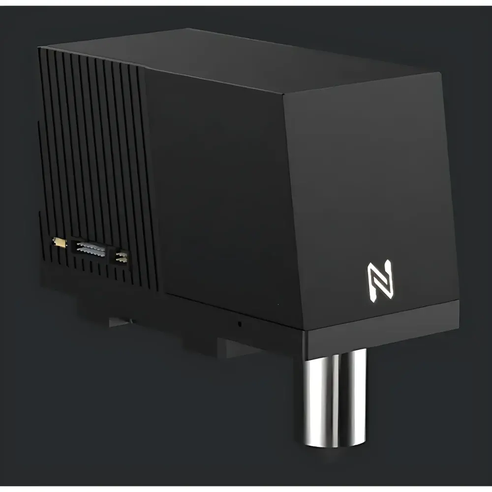
The NILT BEAM Desktop Direct Laser Writing System is a compact, high-precision maskless lithography platform engineered for research laboratories and pilot-line facilities requiring rapid prototyping and low-volume fabrication of micro- and nanoscale structures. Unlike conventional photolithography tools that rely on physical masks, the BEAM system employs focused ultraviolet laser beams—operating at 365 nm, 385 nm, and 405 nm—to directly expose photoresist-coated substrates in a vector-scan mode. Its optical architecture is based on diffraction-limited spot formation (<500 nm FWHM), combined with high-stability galvanometric beam steering and piezo-actuated closed-loop autofocus. This enables deterministic, dose-controlled exposure without proximity gaps or mask alignment overhead. The system supports both single-field writing and seamless tiling across large-area substrates—including full 6-inch wafers—via precision motorized XY stages and sub-pixel stitching algorithms. Designed for integration into cleanroom-adjacent environments, the BEAM maintains metrological traceability to ISO/IEC 17025-aligned calibration protocols and complies with general laboratory safety standards for Class 3B UV laser operation (IEC 60825-1).
Key Features
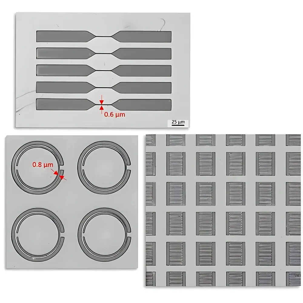
- Sub-500 nm feature resolution achieved through optimized UV laser focusing, dynamic power modulation, and resist-specific dose calibration routines.
- Multi-wavelength UV source (365/385/405 nm) compatible with standard i-line resists (e.g., AZ5214E, SU-8, ma-N) and advanced chemically amplified resists.
- Real-time autofocus subsystem with <1 s response time, utilizing piezoelectric Z-stage control and integrated interferometric height sensing.
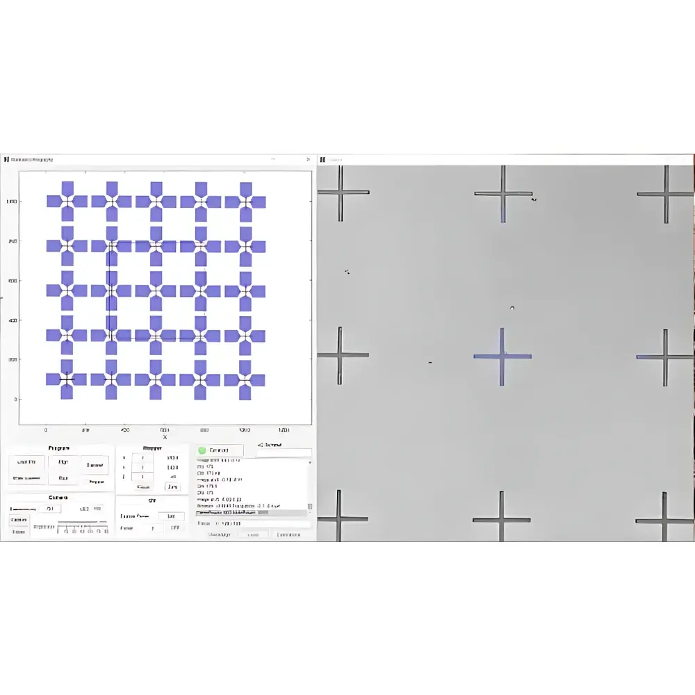
- GDSII-native software interface supporting hierarchical layout import, layer-by-layer alignment visualization, and wafer-level coordinate mapping.
- Automated multi-layer registration with <±200 nm overlay accuracy using fiducial-based image recognition and sub-pixel cross-correlation.
- Tile-based exposure engine enabling uniform patterning over 150 mm × 150 mm areas with <0.5 µm stitching error (RMS).
- Compact footprint (≤0.8 m²) and modular design suitable for Class 1000–10,000 cleanrooms or controlled lab benches.
Sample Compatibility & Compliance
The BEAM system accommodates rigid and semi-rigid substrates including silicon wafers (up to 150 mm diameter), fused silica, quartz, glass, sapphire, and polymer films (e.g., PET, PI). It supports standard spin-coated photoresists (positive and negative tone), as well as emerging materials such as metal-organic frameworks (MOFs) and hybrid sol-gel precursors used in direct laser writing applications. All exposure parameters—including dose, scan velocity, and focus offset—are programmable per layer and region, facilitating process development aligned with ASTM E1994 (Standard Practice for Use of Photoresist Process Control Charts) and ISO 14644-1 cleanroom classification requirements. The system’s control software logs all exposure events with timestamps, operator IDs, and parameter sets, supporting GLP-compliant documentation and audit readiness per FDA 21 CFR Part 11 when configured with electronic signature modules.
Software & Data Management
The BEAM Control Suite is built on a deterministic real-time operating kernel and features a Qt-based GUI with intuitive CNC-style navigation (WASD keys, right-click pan-to-location). It natively imports GDSII, OASIS, and SVG formats, rendering hierarchical layouts with zoomable wafer maps and interactive layer toggling. Critical functions include automatic fiducial detection, batch alignment across multiple dies, and real-time dose compensation based on resist thickness mapping. Export options include TIFF, PNG, and CSV log files compliant with LIMS integration. All user actions, exposure logs, and system diagnostics are stored in encrypted SQLite databases with configurable retention policies, ensuring full traceability for ISO 9001 quality management systems.
Applications
- Photonics: Fabrication of photonic crystals, planar waveguides, microlens arrays, and diffractive optical elements (DOEs) for telecom, LiDAR, and computational imaging systems.
- Microelectronics: Rapid prototyping of MEMS devices (e.g., cantilevers, resonators), RF-IDCs, and test structures for semiconductor process development—especially where mask costs prohibit iterative design cycles.
- Biomedical Engineering: Patterning of biocompatible hydrogels, fabrication of microfluidic channel networks, and surface functionalization templates for biosensor electrode arrays.
- Nanofabrication Research: Direct-write templating for nanoimprint lithography masters, plasmonic antenna arrays, and metamaterial unit cells requiring sub-100 nm placement accuracy.
FAQ
What resist types are validated for use with the BEAM system?
AZ5214E, SU-8 2000 series, ma-N 1400 series, and PMMA are fully characterized; process recipes are available upon request.
Can the BEAM write on non-planar or flexible substrates?
It supports substrates with curvature radii >500 mm and thickness tolerances up to ±25 µm; flatness verification is required prior to exposure.
Is remote operation and monitoring supported?
Yes—via secure SSH tunneling and VNC-enabled GUI access; optional API (Python/C++) allows integration with automated sample handling platforms.
How is calibration maintained over time?
Daily autofocus validation and quarterly beam profile measurements are recommended; NILT provides NIST-traceable calibration kits and service contracts.
Does the system meet regulatory requirements for medical device prototyping?
When deployed with validated SOPs and audit-ready logging, it supports design control documentation under ISO 13485 and FDA QSR guidelines.


