NTT-AT XRESO Series X-ray Resolution Test Chart
| Brand | NTT-AT |
|---|---|
| Origin | Japan |
| Manufacturer Type | Authorized Distributor |
| Product Origin | Imported |
| Model | XRESO Series |
| Component Category | Optical Element |
| Substrate Material | Si / SiN / SiC / Ru |
| Absorber Material | Ta |
| Minimum Feature Size | 20 nm (XRESO-20), 50 nm (XRESO-50HC), 100 nm (XRESO-100) |
| Membrane Thickness | 50 nm–2 µm |
| Substrate Dimensions | 10 mm × 10 mm (standard), customizable |
| Pattern Area | 250 µm × 350 µm to 300 µm² |
| Absorber Thickness | 100 nm–1 µm Ta |
| Alignment | Centered on substrate |
Overview
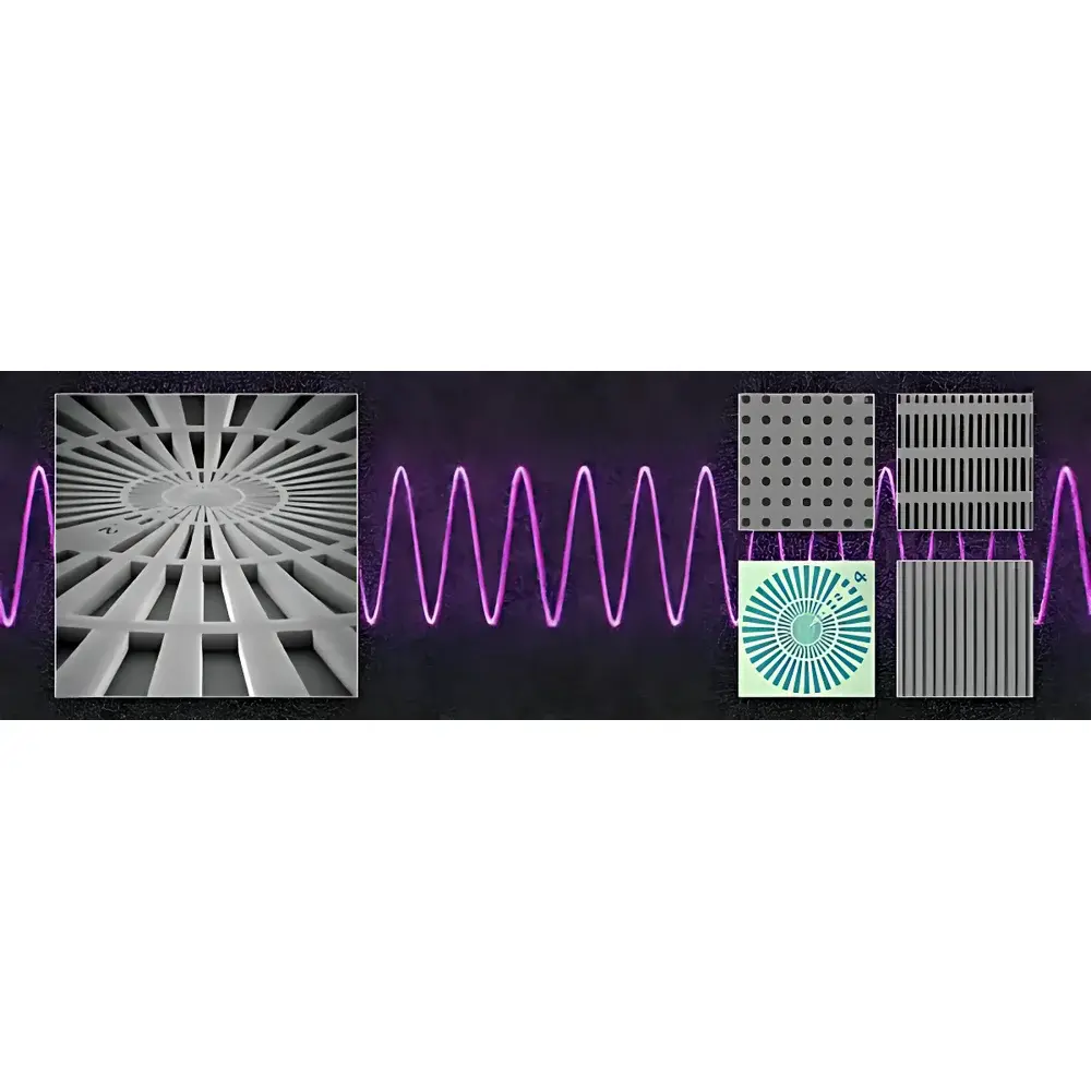
The NTT-AT XRESO Series X-ray Resolution Test Chart is a precision-engineered metrology standard for quantitative assessment of spatial resolution in soft X-ray, extreme ultraviolet (EUV), and XUV optical systems. Designed using lithographically defined tantalum absorbers patterned onto ultra-thin, radiation-resistant membranes—including silicon nitride (SiN), silicon carbide (SiC), and ruthenium-capped silicon—these test charts operate on the principle of edge-spread function (ESF) and line-spread function (LSF) analysis. When illuminated by synchrotron radiation, laser-produced plasma sources, or laboratory-scale X-ray microfocus tubes, the high-contrast, sub-50-nm features enable objective evaluation of modulation transfer function (MTF), point spread function (PSF), and system-level diffraction-limited performance. As the de facto international benchmark adopted by national laboratories (e.g., DESY, ESRF, APS), semiconductor R&D facilities, and university EUV lithography programs, the XRESO series provides traceable, repeatable resolution validation under demanding irradiation conditions.
Key Features
- Three standardized configurations: XRESO-100 (100 nm minimum feature), XRESO-50HC (50 nm L/S with enhanced Ta thickness for improved contrast), and XRESO-20 (20 nm radial and L/S patterns—the highest-resolution commercially available X-ray test chart since 2014)
- Radiation-hardened membrane architectures: SiC (200 nm) and SiN (50–2000 nm) substrates engineered for >109 photons/cm² fluence tolerance at 0.1–2 keV energies
- Atomic-layer precision absorber deposition: Electron-beam evaporated Ta layers with thickness control ±5 nm, minimizing edge roughness (<1.2 nm RMS) critical for MTF fidelity
- Customizable layout and substrate geometry: Pattern field positioning, substrate size (up to 25 × 25 mm), and mounting interface (e.g., kinematic V-groove compatibility) configurable per OEM integration requirements
- Traceable fabrication process: All XRESO charts are manufactured in ISO Class 5 cleanrooms with in-process SEM metrology and post-fabrication CD-SEM certification per NIST-traceable calibration standards
Sample Compatibility & Compliance
The XRESO series is compatible with full-field and scanning X-ray imaging modalities, including zone-plate-based X-ray microscopes, ptychographic coherent diffractive imaging (CDI) setups, grazing-incidence EUV reflectometers, and tabletop X-ray fluorescence (XRF) microprobes. Each chart meets ASTM E2867-22 (Standard Guide for Characterization of X-ray Optics) and ISO 10110-8 (Optics and photonics — Preparation of drawings for optical elements — Part 8: Surface texture specifications) for surface quality and dimensional accuracy. The SiC-based XRESO-20 variant complies with IEC 61228 Annex B for radiation stability in long-duration synchrotron beamline experiments. All products are supplied with individual calibration certificates documenting pattern uniformity, CD deviation (±1.8 nm typical), and membrane integrity verified via helium leak testing (<1×10⁻⁹ mbar·L/s).
Software & Data Management
While the XRESO chart itself is a passive optical standard, its integration into resolution validation workflows is supported by open-format metrology data exchange protocols. Pattern coordinates are delivered in GDSII and OASIS formats for direct import into industry-standard metrology software (e.g., JPK Nanoscope, Zeiss ZEN Blue, or custom Python-based MTF analysis pipelines). NTT-AT provides MATLAB and Python reference scripts for automated LSF extraction, MTF curve fitting (using Wiener filtering and Fourier deconvolution), and uncertainty quantification per ISO/IEC 17025 guidelines. Audit trails for pattern verification—including SEM image timestamps, calibration wafer IDs, and environmental logs—are archived in accordance with GLP-compliant documentation practices and support FDA 21 CFR Part 11 electronic record requirements when deployed in regulated semiconductor process development environments.
Applications
- Quantitative resolution validation of zone plates, multilayer mirrors, and Kirkpatrick-Baez (KB) optics in synchrotron and XFEL beamlines
- MTF characterization of EUV lithography projection optics during mask blank qualification and scanner commissioning
- Benchmarking of ptychographic reconstruction algorithms and phase retrieval fidelity in coherent X-ray imaging
- Calibration of X-ray nanotomography systems used in battery electrode and catalyst pore-structure analysis
- Verification of beamline coherence preservation in X-ray photon correlation spectroscopy (XPCS) and speckle tracking experiments
FAQ
What is the recommended X-ray energy range for optimal contrast with XRESO-20?
XRESO-20 delivers maximum absorption contrast between 0.28 keV (C K-edge) and 0.53 keV (O K-edge); for higher energies (e.g., 1.5–2.5 keV), XRESO-50HC with 500 nm Ta is preferred.
Can the XRESO chart be used in vacuum or UHV environments?
Yes—all variants are baked at 120°C for 24 h and certified for operation in ≤10−9 mbar UHV without outgassing or membrane deformation.
Is there a certified reference material (CRM) designation for XRESO series?
While not an NIST CRM, XRESO charts are supplied with metrology reports traceable to PTB (Physikalisch-Technische Bundesanstalt) reference standards via calibrated CD-SEM.
How is pattern placement accuracy verified?
Each lot undergoes cross-wafer CD-SEM mapping at ≥10 sites; positional accuracy relative to substrate fiducials is guaranteed within ±0.3 µm (3σ).
Do you offer multi-energy or dual-band test charts?
Custom configurations with stacked Ta/Si multilayer absorbers for simultaneous 0.3 keV and 1.0 keV evaluation are available under NRE agreement.


