OETECH 2026SVJ Multi-Beam Confocal Bump Inspection System for Wafer-Level Packaging
| Brand | OETECH |
|---|---|
| Origin | Japan |
| Manufacturer Type | Authorized Distributor |
| Origin Category | Imported |
| Model | 2026SVJ |
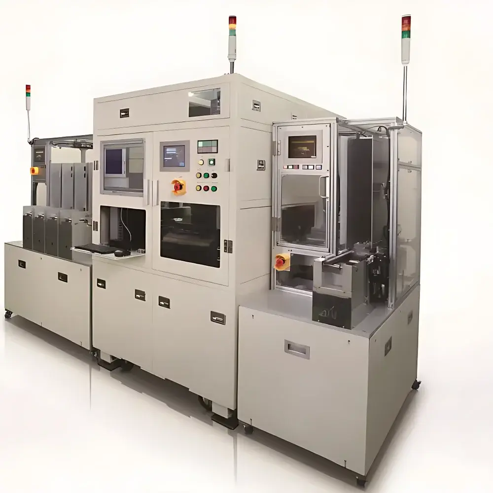
| Dimensions | 2300 mm × 2800 mm × 1640 mm |
| FOV Options | 13×13 mm / 9.9×7.4 mm / 9.9×9.9 mm / 41×33 mm / 15×15 mm |
| XY Positioning Accuracy | 1.4–3.0 µm |
| Z Range | 30–4000 µm |
| Minimum Bump Diameter | 10–100 µm |
| Minimum Bump Pitch | 20–200 µm |
Overview
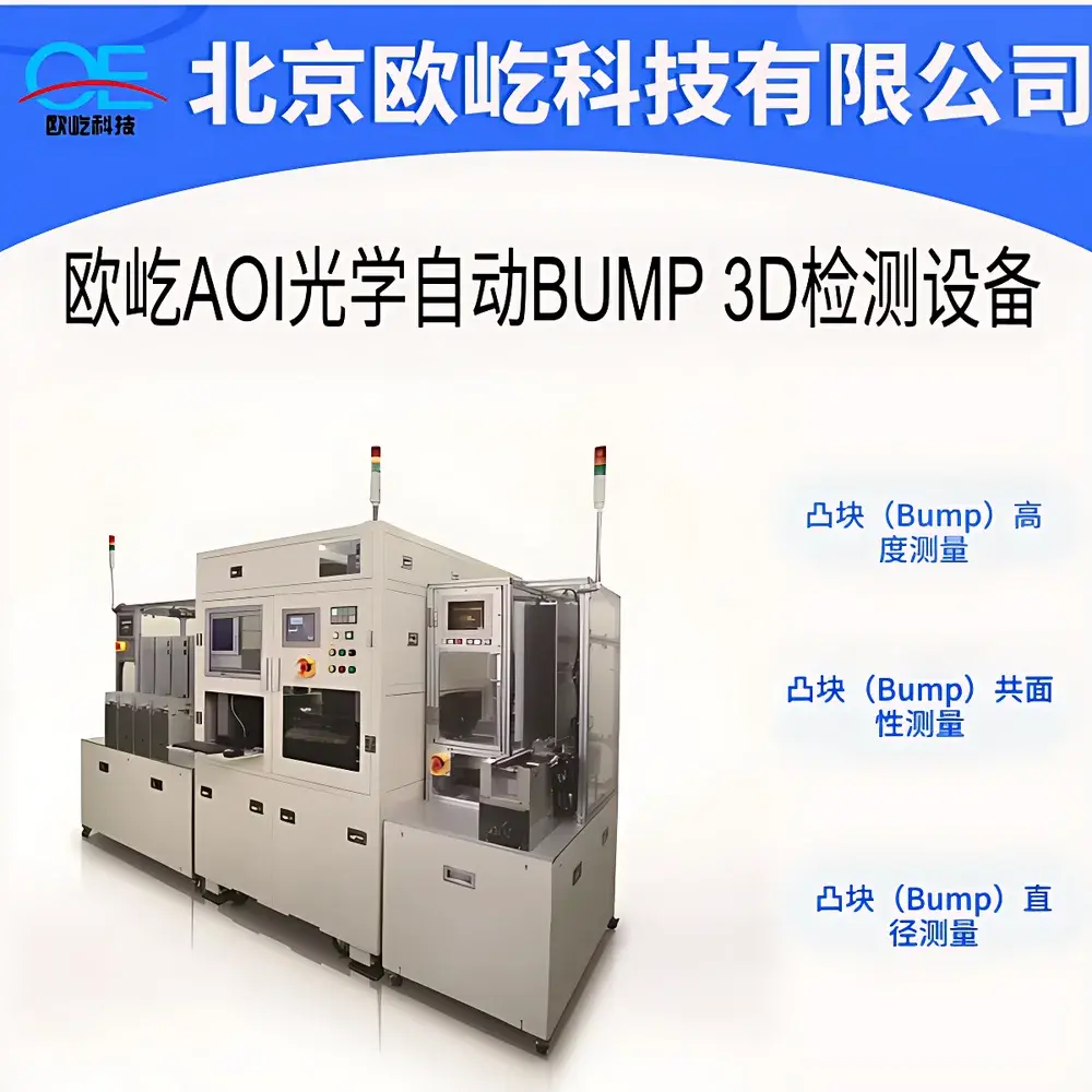
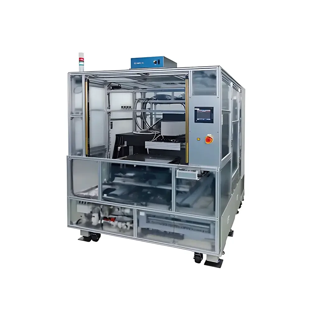
The OETECH 2026SVJ is a high-speed, non-contact 3D metrology system engineered specifically for bump inspection in advanced wafer-level packaging (WLP) and flip-chip interconnect processes. It employs multi-beam confocal optical profiling — a principle grounded in axial chromatic aberration compensation and pinhole-array-based spatial filtering — to deliver nanoscale vertical resolution and sub-micron lateral repeatability without mechanical Z-axis scanning. Unlike conventional confocal systems that rely on piezoelectric or motorized stage movement for focal plane traversal, the 2026SVJ implements a patented gradient-thickness glass disc mechanism. As the disc rotates at controlled angular velocity, radial thickness variation induces precise, continuous optical path difference modulation, enabling real-time Z-focus scanning at speeds exceeding 10 kHz equivalent. This eliminates inertial delay, step-and-settle time, and mechanical wear associated with traditional Z-drives — making the system uniquely suited for inline process monitoring of Cu pillar, solder, and micro-bump arrays on 200 mm to 300 mm wafers.
Key Features
- Multi-beam confocal architecture with >3 million simultaneous detection channels via precision pinhole array — enabling parallel height acquisition across full field-of-view
- Two operational modes: Non-Scanning System (NCS) for maximum throughput (>120 wafers/hour at 10 µm pitch), and Scanning Confocal System (SCS) for enhanced vertical resolution (<5 nm RMS noise floor)
- Gradient-thickness optical disc for inertia-free Z-axis focus modulation — no moving stages in Z-direction; rotational actuation ensures <0.1 ms response time per focal plane
- Configurable FOV options from 9.9×7.4 mm to 41×33 mm, supporting both die-level and full-wafer inspection strategies
- XY stage with air-bearing guidance and laser interferometric feedback — delivering ≤1.4 µm bidirectional repeatability over full travel
- Integrated thermal stabilization and vibration isolation platform compliant with ISO 20484 Class 2 cleanroom environments
Sample Compatibility & Compliance
The 2026SVJ accommodates standard semiconductor substrates including silicon, glass, and organic substrates (ABF, polyimide) with bump diameters ranging from 10 µm to 100 µm and pitches down to 20 µm. It supports both bare-die and packaged units (e.g., fan-out WLP, 2.5D/3D IC stacks) with surface reflectivity spanning 5%–95%. All measurement protocols adhere to ASTM E2923-22 (Standard Guide for Measurement of Bump Height and Coplanarity), ISO/IEC 17025:2017 (for accredited lab use), and are fully compatible with GLP/GMP documentation workflows. Audit trails, electronic signatures, and data integrity controls meet FDA 21 CFR Part 11 requirements when operated with optional validated software modules.
Software & Data Management
The system runs on OETECH BumpVision™ v5.2 — a Windows-based metrology suite featuring automated recipe-driven inspection, real-time coplanarity heatmapping, statistical process control (SPC) dashboards, and defect classification using supervised machine learning models trained on >10⁶ labeled bump profiles. Raw height maps are stored in HDF5 format with embedded metadata (wafer ID, lot number, timestamp, operator, calibration log). Export options include CSV, STEP AP242, and industry-standard SEMI E142 (Equipment Communications Standard) for MES integration. Optional cloud synchronization enables cross-fab comparison and centralized SPC analytics across global manufacturing sites.
Applications
- Quantitative assessment of bump height uniformity and coplanarity for Cu pillar and solder micro-bumps prior to underfill dispensing
- In-process verification of electroplating and reflow parameters during bump formation
- Root cause analysis of voiding, bridging, and incomplete wetting in flip-chip assembly
- Post-reflow inspection for thermal warpage-induced height deviation and shear-induced deformation
- Qualification of redistribution layer (RDL) topography and bump-to-RDL alignment accuracy
- Support for advanced packaging nodes including TSV-based 3D stacking, hybrid bonding, and chiplet integration
FAQ
Does the 2026SVJ require periodic recalibration of the Z-axis optical encoder?
No — the gradient-thickness disc calibration is factory-performed and traceable to NIST standards; drift is <0.02% over 12 months under controlled lab conditions.
Can the system measure bumps on highly reflective or low-reflectivity surfaces without adjustment?
Yes — adaptive gain control and dynamic exposure optimization adjust detector integration time and LED intensity per pixel in real time.
Is the software compatible with existing factory automation infrastructure?
Yes — native support for SECS/GEM, OPC UA, and RESTful API interfaces enables seamless integration with MES, ERP, and yield management platforms.
What is the typical measurement uncertainty for bump height at 20 µm diameter?
Expanded uncertainty (k=2) is ±0.12 µm for 20 µm bumps under ISO 5725-2 repeatability conditions.
How does the system handle wafer bow or tilt during measurement?
Integrated dual-axis capacitive tilt sensors feed real-time corrections to the Z-focus algorithm, maintaining focus lock within ±0.5 µm over ±2 mm wafer warp.


