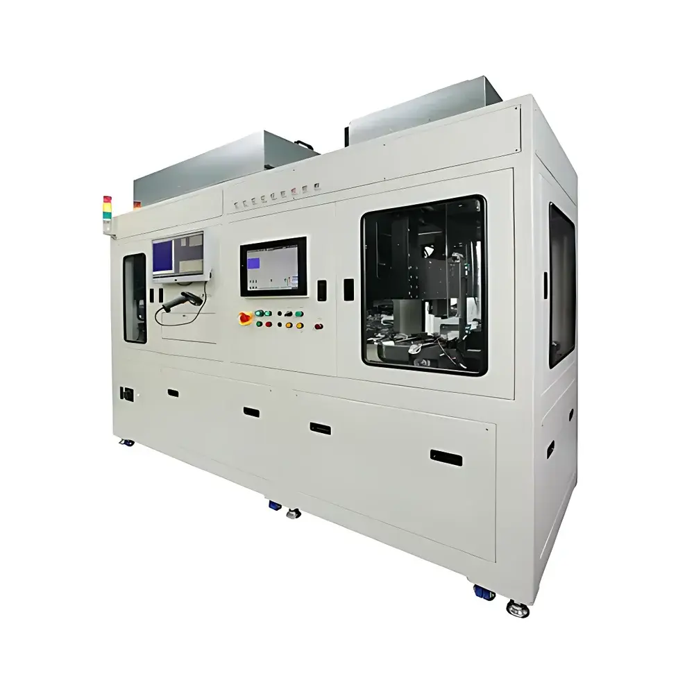
OETECH Bump3D Online Wafer Bump Metrology System
| Brand | OETECH |
|---|---|
| Origin | Japan |
| Manufacturer Type | Authorized Distributor |
| Origin Category | Imported |
| Model | Bump3D Inspection System |
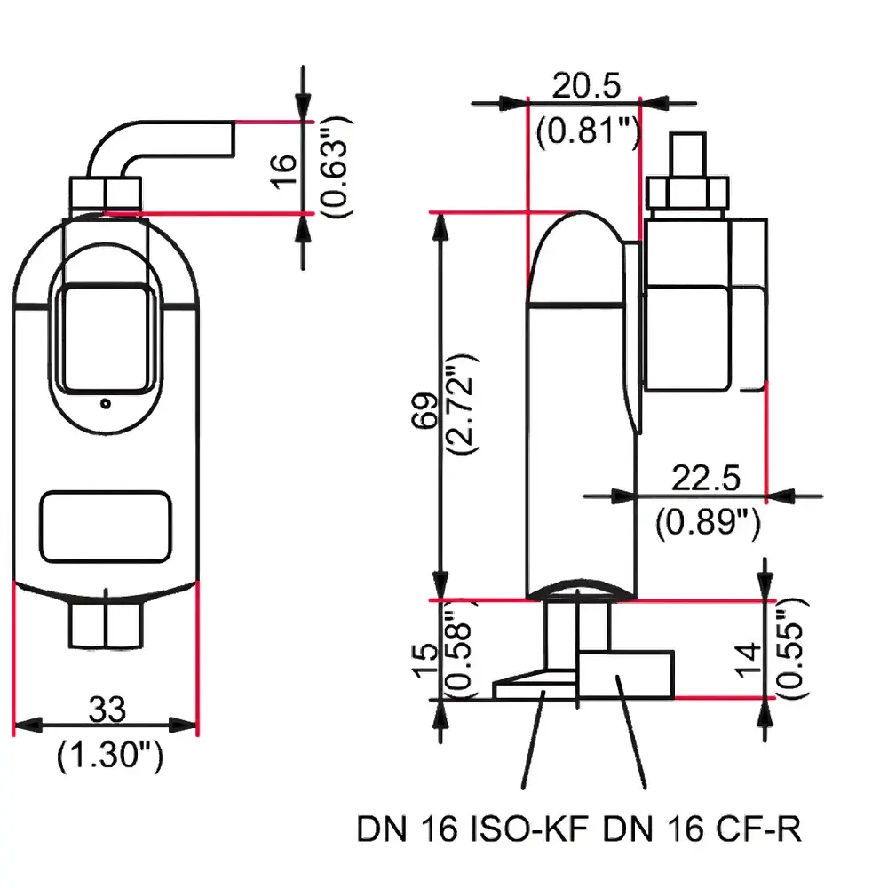
| Dimensions | 2300 mm × 2800 mm × 1640 mm |
| FOV Options | 13×13 mm, 9.9×7.4 mm, 9.9×9.9 mm, 13×13 mm, 41×33 mm, 15×15 mm |
| XY Positioning Accuracy | 1.4–3.0 µm |
| Z Measurement Range | 30–4000 µm |
| Minimum Bump Diameter | 10–100 µm |
| Bump Pitch Resolution | 20–200 µm |
Overview
The OETECH Bump3D Online Wafer Bump Metrology System is a high-precision, non-contact optical metrology platform engineered for real-time, in-line characterization of solder and copper micro-bumps on semiconductor wafers. It employs multi-beam confocal imaging—based on proprietary rotating glass disc focus-tuning—to perform simultaneous height, diameter, and coplanarity measurements without mechanical Z-scanning. Unlike conventional single-beam confocal systems requiring time-consuming axial translation, this architecture achieves sub-millisecond depth sampling by optically shifting the focal plane via calibrated rotation of stacked glass plates. The system is designed for integration into front-end-of-line (FEOL) and bumping process lines, supporting 200 mm, 300 mm, and advanced 450 mm wafer formats with full-field coverage up to 41 mm × 33 mm per acquisition.
Key Features
- Multi-beam confocal sensor with >3 million pinhole points enabling parallel depth sampling across the entire field of view
- Two operational modes: Non-Scanning System (NCS) for throughput-critical applications (up to 60 wafers/hour), and Scanning Confocal System (SCS) for high-resolution metrology (sub-1.4 µm XY accuracy)
- Optical Z-axis modulation via motorized rotating glass disc stack—eliminates piezo or voice-coil Z-stage wear, drift, and hysteresis
- Configurable field-of-view options (from 9.9 × 7.4 mm to 41 × 33 mm) with matched objective lenses and calibration traceability to NIST-traceable step-height standards
- Integrated vibration-isolated granite base and active thermal stabilization (±0.1 °C) to maintain measurement repeatability under factory-floor conditions
- Real-time defect flagging with configurable thresholds for bump height deviation (>±0.5 µm), coplanarity error (>1.2 µm PV), and diameter variation (>±2% nominal)
Sample Compatibility & Compliance
The Bump3D system accommodates bare silicon, low-k dielectric, and redistribution layer (RDL)-processed wafers with bump diameters from 10 µm to 100 µm and pitch down to 20 µm. It supports both solder (SnAg, SnPb) and Cu pillar bumps, including those with under-bump metallization (UBM) layers. Surface reflectivity compensation algorithms mitigate measurement bias across varied metallization stacks (e.g., Ti/Cu/Ni/Au vs. Ti/W/Cu). The platform complies with SEMI E10 (Specification for Definition and Measurement of Equipment Reliability, Availability, and Maintainability), SEMI E142 (Guidelines for Data Collection and Reporting in Semiconductor Manufacturing Equipment), and ISO/IEC 17025:2017 requirements for calibration uncertainty reporting. Full audit trail logging meets FDA 21 CFR Part 11 and EU Annex 11 expectations for regulated environments.
Software & Data Management
OETECH MetroSuite™ v4.2 provides unified control, analysis, and reporting. The software includes automated recipe-based measurement sequencing, SPC charting (X-bar/R, Cpk/Ppk), and spatial heatmap generation for coplanarity deviation mapping. Raw intensity stacks and reconstructed topography data are stored in HDF5 format with embedded metadata (wafer ID, lot number, tool ID, timestamp, environmental conditions). Export modules support industry-standard formats: CSV (for statistical analysis), STEP AP242 (for CAD comparison), and SECS/GEM communication for factory automation integration. All user actions—including parameter edits, calibration updates, and report generation—are logged with digital signature and time-stamped audit trails compliant with GLP and GMP documentation requirements.
Applications
- Process validation and monitoring of electroplated Cu pillar and solder bump formation
- Post-reflow coplanarity verification prior to chip-to-wafer bonding
- Yield analysis correlation between bump geometry deviations and subsequent flip-chip assembly failures
- Qualification of new bumping processes (e.g., micro-bump arrays for 2.5D/3D ICs and HBM interconnects)
- Inline feedback control for plating bath chemistry and current density optimization
- Failure analysis lab use for cross-sectional correlation without destructive sample preparation
FAQ
What is the minimum measurable bump pitch supported by the Bump3D system?
The system resolves bump pitches as low as 20 µm using the high-resolution SCS configuration with 9.9 × 9.9 mm FOV and optimized illumination coherence.
Does the system require periodic recalibration with physical step standards?
Yes—calibration is performed using NIST-traceable fused silica step-height artifacts (100 nm to 5 µm steps); recommended frequency is every 24 hours for production environments or after any mechanical disturbance.
Can the Bump3D interface with MES or host factory automation systems?
Yes—it supports SECS/GEM over TCP/IP and provides RESTful API endpoints for real-time data ingestion into manufacturing execution systems.
Is the optical design compatible with low-reflectivity UBM layers such as TiW or TaN?
Yes—adaptive illumination intensity control and polarization-resolved signal processing ensure stable focus detection across reflectivity ranges from 5% (TiW) to 95% (Au-plated bumps).
How is measurement uncertainty quantified and reported?
Uncertainty budgets follow ISO/IEC Guide 98-3 (GUM), incorporating contributions from optical aberration, thermal expansion, stage positioning error, and detector noise; typical expanded uncertainty (k=2) is ±0.35 µm for height and ±0.8 µm for coplanarity over 10 mm × 10 mm regions.