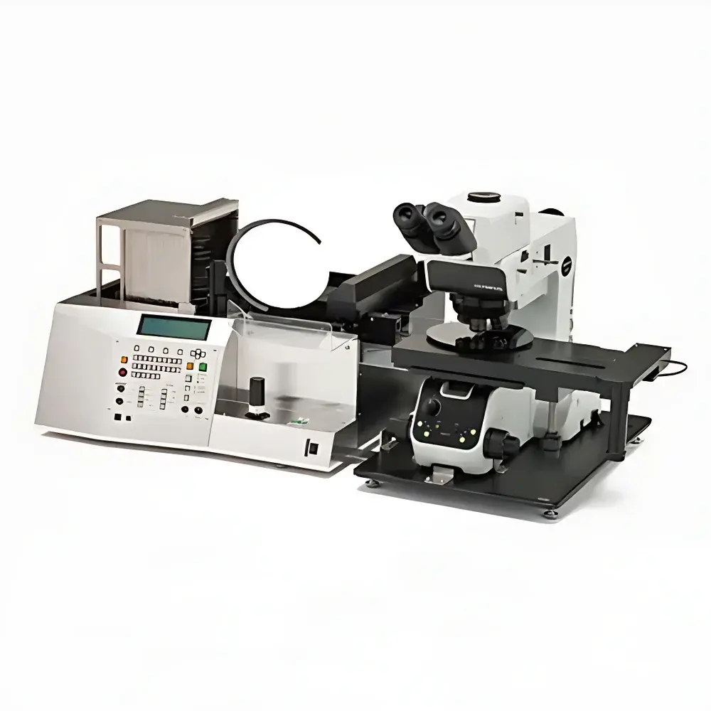
OLYMPUS AL120 Wafer Handler
| Brand | Olympus |
|---|---|
| Origin | Japan |
| Manufacturer Type | Authorized Distributor |
| Origin Category | Imported |
| Model | AL120 |
| Pricing | Upon Request |
Overview
The OLYMPUS AL120 Wafer Handler is an engineered automation module designed for precise, non-contact transfer of silicon and compound semiconductor wafers—from standard FOUPs, SMIF pods, or open cassettes—onto the stage of high-resolution inspection microscopes, particularly the OLYMPUS MX63 and MX61L semiconductor inspection platforms. Built upon a kinematic foundation of repeatability and contamination control, the AL120 operates on a hybrid pneumatic-electromechanical actuation architecture, integrating real-time positional feedback and optical alignment verification to ensure sub-millimeter placement accuracy across wafer diameters up to 200 mm. Its core function is not merely mechanical handling but process-integrated metrology readiness: every transfer cycle preserves wafer surface integrity, maintains orientation fidelity (notch/flat detection), and enables immediate transition into macroscopic top/bottom inspection without manual repositioning.
Key Features
- Three configurable variants: AL120-200 (200 mm fixed), AL120-150/200 (field-convertible), and AL120-150 (≤150 mm optimized)
- Ultra-thin wafer compatibility: AL120-LMB-90 variant supports full-cassette handling of 90 µm wafers with reinforced cantilever arms and low-acceleration lift profiles
- 360° motorized wafer rotation for comprehensive macro inspection of both frontside and backside surfaces
- Integrated joystick-controlled tilt mechanism (±15°) during top-side macro imaging to optimize defect contrast under oblique illumination
- 10 programmable recipe slots—each storing cassette type, wafer diameter, notch orientation, transfer velocity profile, and vacuum sequencing parameters
- Non-contact optical centering using dual-axis laser triangulation sensors; notch/flat identification via monochrome CMOS edge-detection imaging
- Triple-redundant wafer presence monitoring (top, mid, and base sensor zones) to prevent multi-wafer pickup, cross-slot retrieval, or stage collision
- Real-time LCD interface displaying active recipe ID, current wafer position status, vacuum pressure, and alignment error margin (±0.15 mm typical)
Sample Compatibility & Compliance
The AL120 accommodates standard SEMI-compliant wafer formats including 100 mm, 125 mm, 150 mm, and 200 mm diameters, with optional adaptability for 76.2 mm (3-inch) substrates upon custom bracket integration. It supports bare silicon, SOI, GaAs, SiC, and GaN wafers with thicknesses ranging from 50 µm to 1000 µm. All motion control firmware complies with SEMI E10 (Definition and Measurement of Equipment Reliability and Availability) and SEMI E19 (Equipment Communication Standard). Mechanical design adheres to ISO 14644-1 Class 5 cleanroom requirements when operated within laminar flow hoods or mini-environments. Vacuum system components meet FDA 21 CFR Part 11 traceability standards for audit logging of critical handling events.
Software & Data Management
The AL120 operates via embedded ARM Cortex-M7 controller firmware with deterministic real-time scheduling (RTOS). Recipe data—including cassette geometry definitions, wafer dimensional tolerances, and sequence logs—is stored in encrypted EEPROM with write-cycle redundancy. Optional Ethernet/IP or RS-232 connectivity enables integration into factory MES systems for SPC-triggered event logging (e.g., “wafer misalignment >0.2 mm” or “vacuum decay >50 mbar/s”). All operational timestamps, sensor readings, and manual override actions are retained for ≥30 days and exportable as CSV or XML for GLP/GMP documentation workflows. No proprietary software installation is required on host PCs; configuration is performed exclusively through the front-panel interface or optional OLYMPUS Stream™ Semiconductor Edition plugin (v3.5+).
Applications
- Front-end wafer fab: post-lithography particle inspection, CMP residue mapping, and edge bead removal verification
- Back-end packaging: die attach inspection, wire bond pad cleanliness assessment, and mold compound void detection
- R&D laboratories: comparative analysis of epitaxial layer uniformity, defect clustering statistics, and thin-film stress-induced warpage quantification
- Failure analysis labs: rapid staging of suspect wafers for cross-sectional SEM correlation or FIB-SEM site targeting
- Quality assurance: incoming material inspection per ASTM F122–22 (Standard Specification for Silicon Wafers for Integrated Circuits)
FAQ
Does the AL120 support automated integration with third-party microscopes beyond OLYMPUS MX series?
Yes—custom mechanical and electrical interfaces (including TTL trigger I/O, analog position feedback, and RS-485 command protocol mapping) are available under NDA for integration with Zeiss Axio Imager, Nikon Eclipse LV100ND, or Keyence VHX-series platforms.
What is the maximum allowable wafer warp for reliable handling by the AL120?
The system is validated for wafers with total indicator reading (TIR) ≤ 30 µm at 200 mm diameter; higher warp values require AL120-LMB-90 configuration with adaptive grip compensation.
Is notch detection performed before or after wafer lifting from the cassette?
Notch/flat recognition occurs during the pre-lift optical scan phase—prior to vacuum engagement—to avoid mechanical strain on warped or fragile substrates.
Can the AL120 be retrofitted with robotic arm coupling for cluster tool integration?
Standard AL120 units do not include SECS/GEM interfaces; however, OLYMPUS offers the AL120-RM variant with SEMI E30/E40-compliant hardware abstraction layer and SECS-II message parsing firmware.
How is calibration maintained over extended operation in high-throughput environments?
The system performs automatic self-calibration of optical centering sensors every 24 hours or after 500 transfer cycles, referencing internal ceramic fiducials traceable to NIST SRM 2095a.


