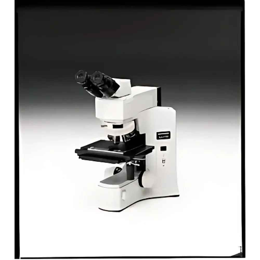
OLYMPUS BX41M-LED Metallurgical Microscope for ESD-Safe Microelectronics Inspection
| Brand | OLYMPUS |
|---|---|
| Origin | Japan |
| Model | BX41M-LED |
| Optical System | UIS2 Infinity-Corrected |
| Observation Modes | Brightfield, Simple Polarization, Differential Interference Contrast (DIC) |
| Illumination | 3 W White LED Reflected Light Only |
| Objective Turret | Manual 5- or 6- or 7-Position (ESD-Compatible) |
| Focusing | Coaxial Manual, 35 mm Travel, 0.1 mm/rev Fine Focus |
| Max. Specimen Height | 65 mm |
| Stage | Right- or Left-Handed Mechanical Stage (76 × 52 mm or 100 × 105 mm XY Travel) |
| Eyepiece Field Number | 22 (Widefield) or 26.5 (Ultra-Widefield) |
| Dimensions (W×D×H) | 283 × 455 × 480 mm |
| Weight | 14 kg |
Overview
The OLYMPUS BX41M-LED is a high-performance, ESD-safe metallurgical microscope engineered specifically for precision inspection and failure analysis in microelectronics manufacturing, semiconductor packaging, PCB assembly, and advanced materials R&D. Designed around the UIS2 (Universal Infinity System) optical platform, it delivers diffraction-limited resolution, exceptional flat-field correction, and chromatic fidelity across all observation modes—brightfield (BF), simple polarization (POL), and differential interference contrast (DIC). Unlike conventional halogen-illuminated metallurgical systems, the BX41M-LED integrates a 3 W white LED illumination module with built-in electrostatic discharge (ESD) protection circuitry, eliminating static buildup on optical components and stage surfaces—a critical requirement when handling bare wafers, flip-chip assemblies, or static-sensitive IC substrates. The LED source operates at constant color temperature (~5700 K), ensuring photometric stability over its rated lifetime (>25,000 hours), independent of intensity adjustment or aging—thereby preserving quantitative image consistency for comparative metrology and documentation workflows.
Key Features
- ESD-compliant mechanical design: Conductive coatings on turret, stage, and illumination housing; grounded chassis architecture compliant with ANSI/ESD S20.20 and IEC 61340-5-1 standards.
- Dual-reflection illumination options: BX-KMA-LED (standard brightfield) and BX-AKMA-LED (with integrated oblique illumination mechanism), enabling rapid contrast enhancement without external accessories or alignment recalibration.
- Modular UIS2 optical path: Supports interchangeable objective turrets—including 5-position BF-only, 6-position BF/DIC, and 7-position BF/DIC configurations—all rated for ESD compatibility and certified for use with strain-free, semi-apochromatic metallurgical objectives (e.g., LMPLFLN series).
- High-precision manual focusing system: 35 mm vertical travel with dual coarse/fine coaxial controls; fine focus calibrated to 0.1 mm per revolution, providing tactile repeatability essential for focus-stacking and depth-profiling applications.
- Thermally stable LED illumination: Power consumption ≤0.43 W (equivalent to 1/7 that of a 30 W halogen lamp); zero warm-up time, no UV/IR emission, and negligible heat transfer to specimens—critical for thermally sensitive solder joints or polymer encapsulants.
Sample Compatibility & Compliance
The BX41M-LED accommodates specimens up to 65 mm in height, supporting standard 4-inch wafers, BGA packages, ceramic substrates, and cross-sectioned metallographic mounts. Its open-stage architecture allows integration with optional micromanipulators, probe stations, or environmental chambers (subject to third-party certification). All optical and mechanical components meet ISO 9022-1 (optical instruments — environmental testing) and JIS B 7153 (metallurgical microscopes — performance requirements). The system supports GLP-compliant documentation when paired with Olympus cellSens software and an FDA 21 CFR Part 11–enabled imaging workstation (audit trail, electronic signatures, user access control).
Software & Data Management
When interfaced with Olympus cellSens digital imaging software (v2.4 or later), the BX41M-LED enables automated acquisition of multi-focus Z-stacks, DIC vector mapping, polarization angle calibration, and real-time measurement annotation (line, area, particle count). Raw image data is stored in TIFF or Olympus OIF format with embedded metadata—including objective magnification, illumination mode, exposure parameters, and stage coordinates—ensuring traceability under ISO/IEC 17025 and ASTM E2015 guidelines. Optional modules support batch report generation aligned with IPC-A-610 or JEDEC J-STD-001 inspection criteria.
Applications
- Fault isolation in wafer-level packaging (WLP) and fan-out wafer-level packaging (FOWLP)
- Intermetallic compound (IMC) thickness measurement at solder joint interfaces
- Crack propagation analysis in thin-film metallization layers
- Surface contamination identification via oblique-illumination-enhanced topography contrast
- Qualitative birefringence assessment of stress-induced anisotropy in die attach epoxies
- Process validation for plasma etch uniformity and CMP endpoint detection
FAQ
Is the BX41M-LED compatible with DIC accessories from older BX series models?
Yes—the UIS2 optical path maintains mechanical and optical backward compatibility with DIC sliders, prisms, and condensers designed for BX51/BX61 platforms, provided they are ESD-certified versions.
Can transmittance observation be added to this model?
No—the BX41M-LED is configured exclusively for reflected-light microscopy. For combined BF/DIC/POL + transmitted-light capability, consider the BX43 or BX53 platform with dual-path illumination base.
What is the maximum usable magnification with the standard 10× widefield eyepieces?
With a 50× metallurgical objective (NA 0.75), the system achieves effective magnification of 500× while maintaining >180 µm depth of field—sufficient for grain boundary delineation and solder void characterization per IPC-TM-650 2.1.1.
Does the LED illumination support intensity modulation for quantitative reflectance analysis?
Yes—intensity is digitally controllable from 1% to 100% in 0.1% increments via the front-panel encoder or cellSens interface, with linearity deviation <±2% across full range (calibrated per CIE 15:2018).


