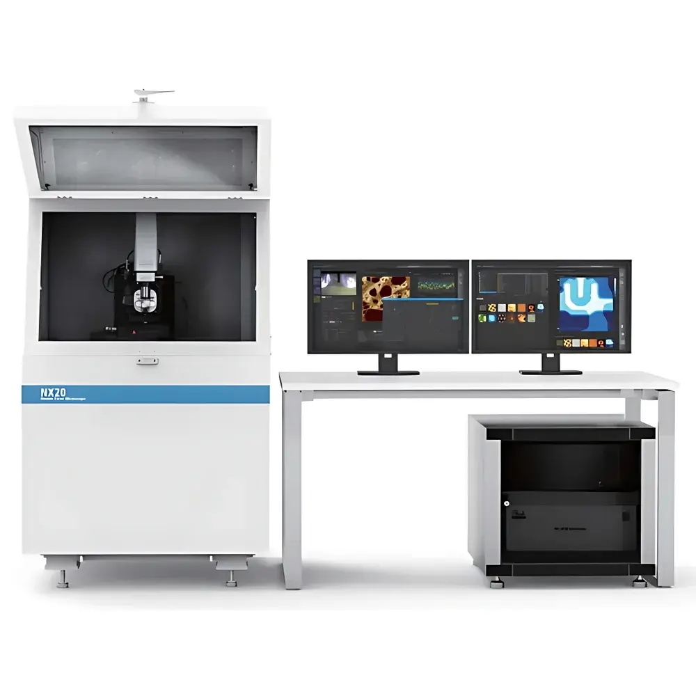
Park NX20 Atomic Force Microscope
| Origin | South Korea |
|---|---|
| Manufacturer Type | Authorized Distributor |
| Origin Category | Imported |
| Model | NX20 |
| Price Range | USD 195,000 – 260,000 (FOB) |
| Instrument Type | Atomic Force Microscope |
| Application Class | Materials Science AFM |
| XY Positional Noise | < 0.25 nm (over 80 µm scan range) |
| Z-Noise Floor | < 0.03 nm |
| Feedback Loop Bandwidth | > 9 kHz |
| Maximum Sample Diameter | 200 mm |
| XY Scan Range | 100 µm × 100 µm |
| Z Scan Range | 15 µm (extendable to 30 µm) |
| Control Software | Park SmartScan™ Automation Suite |
Overview
The Park NX20 Atomic Force Microscope is a high-precision, materials-focused scanning probe microscope engineered for quantitative nanoscale surface characterization in research and industrial metrology environments. Utilizing a true non-contact tapping mode architecture with closed-loop piezoelectric positioning and a low-drift, ultra-low-noise Z-sensor design, the NX20 delivers traceable topographic data without tip-sample convolution artifacts, piezoelectric creep, or overshoot-induced height distortion. Its core measurement principle relies on optical beam deflection detection of cantilever oscillation amplitude and phase shifts—enabling simultaneous acquisition of topography, adhesion, stiffness, and dissipation maps at sub-nanometer vertical resolution. Designed specifically for semiconductor process control, failure analysis, and advanced materials R&D, the NX20 meets the stringent repeatability and stability requirements of ISO/IEC 17025-accredited labs and GLP-compliant workflows.
Key Features
- True non-contact operation with forward/backward lateral drift < 0.15% — eliminating scan-direction bias in critical dimension metrology.
- Ultra-low Z-noise floor (< 0.03 nm RMS) achieved via proprietary interferometric Z-detection, enabling accurate quantification of atomic-step heights and monolayer-thick films.
- High-bandwidth feedback loop (> 9 kHz) supporting stable imaging at scan speeds up to 2 Hz over 100 µm × 100 µm fields — essential for throughput-sensitive inline QA/QC applications.
- Integrated 200 mm motorized sample stage with automated alignment and multi-point mapping capability — compatible with wafers from 50 mm (2″) to 200 mm (8″), including full-reticle mask inspection setups.
- Patented flat-scanner architecture with no mechanical hysteresis — ensuring geometric fidelity and pixel-accurate registration across repeated scans.
- SmartTip™ longevity optimization algorithm extends probe lifetime by ≥10× versus conventional contact-mode AFMs, reducing consumables cost and downtime in high-volume defect review.
Sample Compatibility & Compliance
The NX20 accommodates rigid and semi-rigid samples up to 200 mm in diameter and 25 mm in thickness, including silicon, GaAs, InP, SiC, GaN wafers; MEMS devices; magnetic thin films; biological substrates (e.g., mica-supported lipid bilayers); and polymer composites. All scanning modes comply with ASTM E2533–22 (Standard Guide for AFM Measurements) and support traceable calibration using NIST-traceable step-height standards. The system architecture is fully compatible with FDA 21 CFR Part 11 requirements when deployed with audit-trail-enabled SmartScan™ software configuration and networked user authentication — making it suitable for regulated environments including semiconductor fab metrology labs and medical device material qualification.
Software & Data Management
Park SmartScan™ is a modular, Windows-based control and analysis platform offering real-time parameter optimization, scriptable automation (Python API), and batch-processing pipelines for large-area stitching, roughness statistics (Sa, Sq, Sz per ISO 25178), and cross-sectional profiling. Raw data are stored in vendor-neutral .spm format (compatible with Gwyddion, MountainsMap®, and SPIP), while processed reports export to PDF, CSV, and TIFF with embedded metadata (timestamp, operator ID, calibration certificate ID). Audit trail logging records all parameter changes, scan start/stop events, and user logins — satisfying GLP/GMP documentation requirements. Optional modules include Conductive AFM (CAFM), Kelvin Probe Force Microscopy (KPFM), and Magnetic Force Microscopy (MFM) extension kits with dedicated calibration routines.
Applications
- Semiconductor manufacturing: gate oxide thickness uniformity, trench depth metrology, CMP endpoint detection, DRAM capacitor sidewall angle analysis.
- Failure analysis: interconnect voiding, dielectric cracking, ESD damage localization, and nanoscale corrosion mapping on packaged ICs.
- Advanced materials: 2D material layer counting (graphene, MoS₂), ferroelectric domain imaging, piezoelectric coefficient mapping.
- Life sciences: amyloid fibril morphology, virus particle height distribution, cell membrane elasticity (via force spectroscopy).
- Energy research: solid-electrolyte interface (SEI) layer evolution in battery anodes, catalyst nanoparticle sintering kinetics.
- Quantum device development: superconducting qubit substrate roughness screening, topological insulator surface state correlation with atomic terraces.
FAQ
Does the NX20 support vacuum or liquid imaging environments?
Yes — optional environmental chambers enable controlled atmosphere (N₂, Ar), liquid cell (electrochemical AFM), and low-vacuum operation (down to 10⁻² mbar) without hardware modification.
Is the system compatible with third-party probes?
The NX20 accepts standard 125 µm-wide rectangular cantilevers (e.g., Bruker, NanoAndMore, Olympus) via its universal holder; Park-certified probes are recommended for guaranteed noise performance and calibration traceability.
Can the NX20 perform nanomechanical property mapping beyond topography?
Yes — integrated force-distance spectroscopy, PeakForce QNM®, and contact resonance modes enable quantitative modulus, adhesion, and loss tangent mapping at pixel resolution down to 5 nm.
What level of training and service support is provided?
Park Systems offers on-site installation, 5-day operator certification, and annual preventive maintenance contracts with remote diagnostics and firmware update management.
How is data integrity ensured during long-duration scans?
The system employs real-time thermal drift compensation, active acoustic isolation (integrated passive air table + optional active damping), and continuous Z-sensor recalibration every 30 seconds to maintain sub-0.1 nm height stability over 4+ hour acquisitions.


