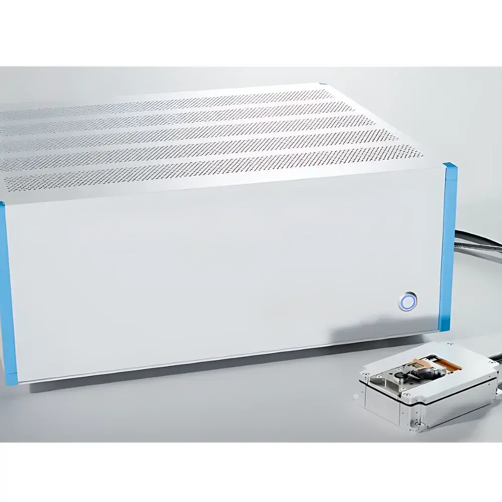
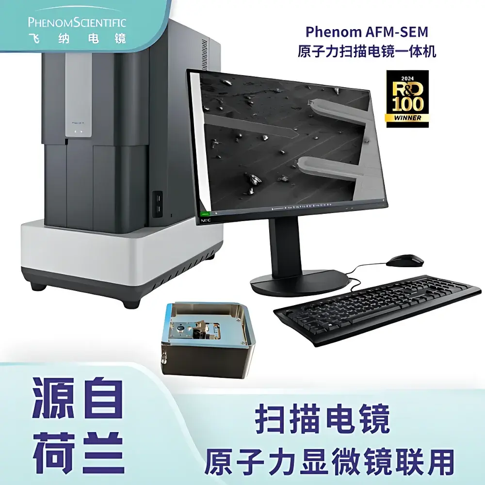
Phenom AFM-SEM Integrated Atomic Force and Scanning Electron Microscope
| Brand | Phenom |
|---|---|
| Origin | Netherlands |
| Model | Phenom AFM-SEM |
| Instrument Type | Benchtop SEM-AFM Hybrid System |
| Electron Source | Cerium Hexaboride (CeB₆) |
| Maximum Sample Dimensions | 21 mm × 11 mm × 8 mm |
| Scan Range (Open-Loop) | 100 µm × 100 µm × 20 µm |
| Scan Range (Closed-Loop) | 80 µm × 80 µm × 16 µm |
| Spatial Resolution | 0.2 nm (lateral) × 0.04 nm (vertical) |
| Sample Mass Limit | 100 g |
| Imaging Modes | Topography & Roughness, Conductive AFM (CAFM), Kelvin Probe Force Microscopy (KPFM), Magnetic Force Microscopy (MFM), Piezoresponse Force Microscopy (PFM), Electrostatic Force Microscopy (EFM), Force–Distance (F–z) Curves, Current–Voltage (I–V) Spectroscopy |
Overview
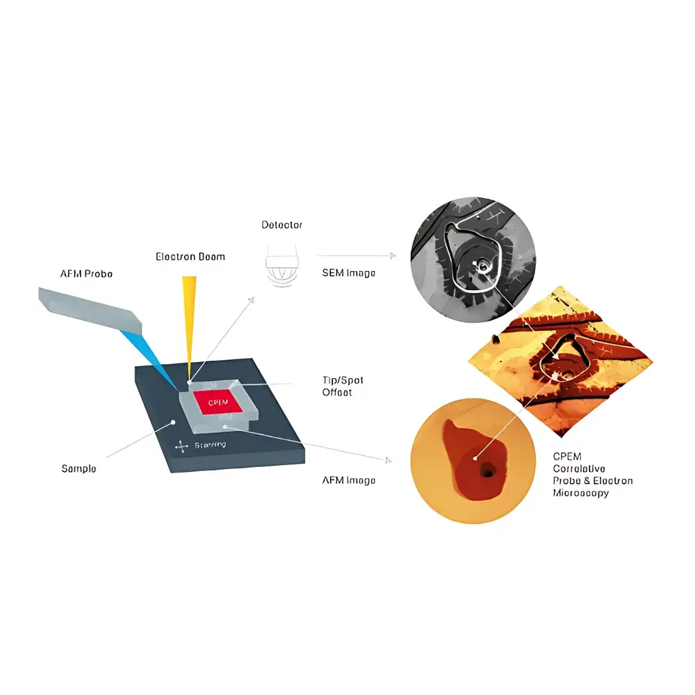
The Phenom AFM-SEM is a fully integrated benchtop hybrid instrument that co-localizes high-resolution scanning electron microscopy (SEM) and atomic force microscopy (AFM) within a single vacuum-compatible platform. Engineered for correlative nanoscale characterization, it enables simultaneous or sequential acquisition of topographic, compositional, electrical, magnetic, and mechanical property data from the same region of interest—without sample transfer or repositioning. The system employs a thermally stable CeB₆ electron source to deliver high-brightness, low-noise imaging at accelerating voltages up to 15 kV, while its closed-loop piezoelectric scanner ensures sub-nanometer positional fidelity in all three axes. Unlike conventional post-acquisition overlay methods, this hardware-synchronized architecture guarantees pixel-perfect spatial registration between SEM secondary electron (SE) images and AFM-derived quantitative surface maps—critical for failure analysis, thin-film metrology, and functional material studies.
Key Features
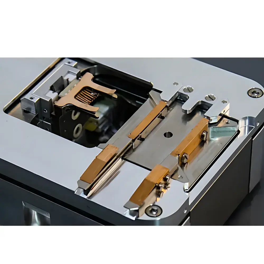
- Benchtop form factor with integrated vacuum chamber (base pressure <10⁻⁴ Pa), eliminating need for dedicated SEM rooms or external vibration isolation tables
- Hardware-synchronized SEM-AFM acquisition enabling real-time cross-modal navigation: SEM image guides AFM probe positioning; AFM height map updates SEM stage coordinates
- Closed-loop XYZ piezoscanner with 80 µm × 80 µm × 16 µm scan range and <0.04 nm vertical resolution, calibrated via on-chip interferometric feedback
- Dual-mode detection: SE/BSE imaging (1–15 kV) combined with multi-frequency AFM modalities including CAFM, KPFM, PFM, MFM, and EFM
- Automated tip approach and force curve acquisition with programmable setpoint control (0.1–100 nN) and real-time deflection monitoring
- Modular cantilever compatibility: supports standard silicon, conductive Pt/Ir, and ferromagnetic tips (resonance frequency 15–300 kHz)
Sample Compatibility & Compliance
The Phenom AFM-SEM accommodates samples up to 21 mm × 11 mm × 8 mm and 100 g mass, supporting both conductive and non-conductive specimens without mandatory metal coating—enabled by low-voltage SEM operation and charge compensation algorithms. It complies with IEC 61000-4-2 (ESD immunity) and meets CE/UKCA safety directives for laboratory equipment. Data integrity protocols align with GLP and GMP requirements: audit trails log user actions, parameter changes, and calibration events; raw AFM force curves and SEM detector gain settings are stored with metadata in vendor-neutral HDF5 format. While not FDA 21 CFR Part 11–certified out-of-the-box, the software architecture supports integration with validated LIMS environments through API-driven export workflows.
Software & Data Management
Phenom’s proprietary Phenom Desktop Software v5.x provides unified control of both SEM and AFM subsystems via a single GUI. All imaging modes—including KPFM surface potential mapping and PFM hysteresis loop acquisition—are accessible through context-aware wizards with preconfigured presets for common materials (e.g., graphene, perovskites, polymer blends). Quantitative analysis modules include ISO 25178-compliant roughness parameters (Sa, Sq, Sdr), current density mapping (nA/µm²), and piezoelectric coefficient extraction (pm/V). Export options include TIFF, PNG, CSV, and MATLAB-compatible .mat files. Batch processing scripts can be authored in Python using the documented SDK, enabling automated measurement sequences across multiple samples under identical conditions.
Applications
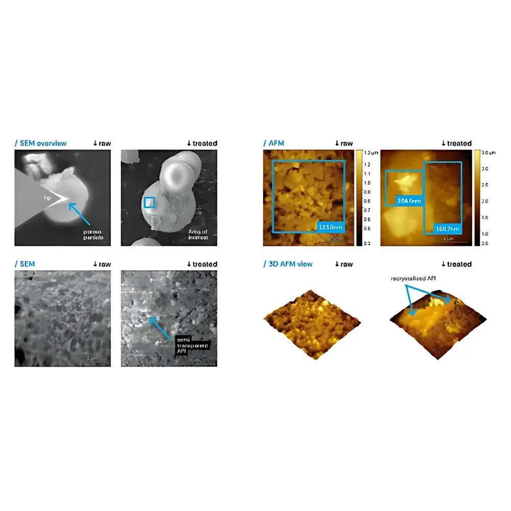
- Correlative defect analysis in semiconductor packaging: SEM identifies voids or delamination; AFM quantifies interfacial roughness and local conductivity at solder joint interfaces
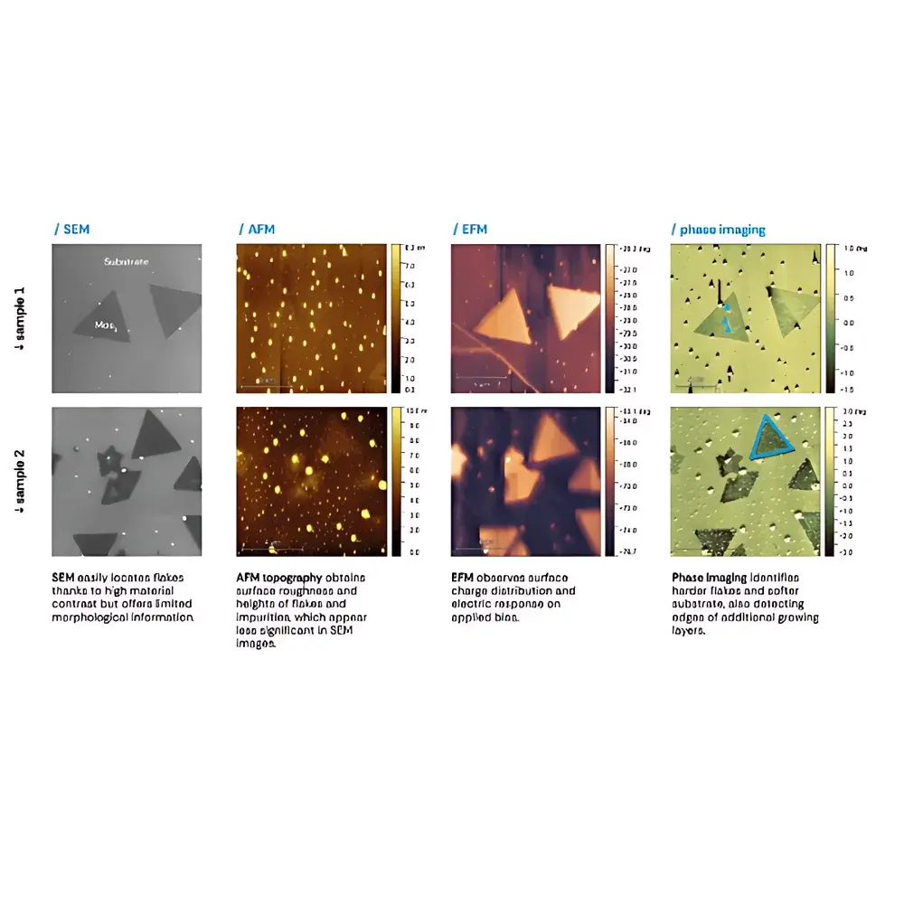
- 2D material characterization: Simultaneous graphene layer counting (via SE contrast) and nanomechanical modulus mapping (via contact resonance AFM)
- Ferroelectric domain dynamics: PFM phase/amplitude loops synchronized with in situ thermal drift correction from SEM stage temperature sensors
- Biopolymer nanostructure validation: AFM-based Young’s modulus distribution overlaid onto SEM-immunolabeled extracellular matrix fibrils
- Energy storage electrode degradation: Post-cycling cathode particles imaged in SEM for morphology; same locations probed via CAFM to map Li-ion diffusion barriers
FAQ
Is vacuum required for AFM operation?
Yes—the AFM module operates inside the same vacuum chamber as the SEM to eliminate acoustic noise and thermal drift; typical operating pressure is 10⁻³–10⁻⁴ Pa.
Can the system perform in situ electrical biasing during imaging?
Yes—integrated biasing stages support DC and AC voltage application (±20 V, 1 MHz bandwidth) to samples during both SEM and AFM acquisition.
What is the typical time required to switch between SEM and AFM modes?
Mode switching is software-initiated and takes <90 seconds, including beam blanking, probe approach, and laser alignment verification.
Are third-party AFM probes compatible?
All standard 125 µm × 125 µm × 500 µm rectangular silicon cantilevers with reflective coating are mechanically and optically compatible; electrical calibration requires vendor-provided reference standards.
Does the system support automated feature recognition and targeted AFM scanning?
Yes—using machine learning–enhanced pattern recognition in SEM images, users can define regions of interest (ROIs) for autonomous AFM rastering with sub-micron targeting accuracy.


