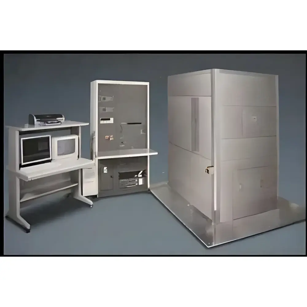
PHI 700 SAM Auger Electron Spectrometer
| Origin | Japan |
|---|---|
| Manufacturer Type | Authorized Distributor |
| Origin Category | Imported Instrument |
| Model | PHI 700 SAM |
| Price | Upon Request |
| Detection Limit | 0.1 at.% |
| Minimum Probe Spot Size | 6 nm |
| Information Depth | ≤ 5 nm |
| Elemental Coverage | All elements except H and He |
Overview
The PHI 700 Scanning Auger Microprobe (SAM) is a high-performance surface analytical instrument engineered for quantitative elemental characterization, spatially resolved chemical mapping, and depth-profiling of solid materials at the nanoscale. Based on the physical principle of Auger electron spectroscopy (AES), the system detects energy-resolved electrons emitted from the top 0.5–5 nm of a sample surface following primary electron beam excitation. Unlike X-ray photoelectron spectroscopy (XPS), AES offers superior spatial resolution—down to 6 nm in optimized conditions—and higher surface sensitivity for light elements (Li through U), excluding only hydrogen and helium. The PHI 700 integrates a field-emission electron gun, ultra-high vacuum (UHV) environment (<5×10⁻¹⁰ Torr), and multi-channel hemispherical analyzer to deliver high signal-to-noise ratio spectra with excellent energy resolution (≤0.3% at E₀ = 1 keV). Designed for rigorous R&D and failure analysis workflows in microelectronics, metallurgy, catalysis, and thin-film development, the instrument meets the stringent requirements of industrial QA/QC laboratories and academic surface science facilities.
Key Features
- Nanometer-scale spatial resolution: 6 nm minimum probe diameter enables sub-feature analysis of integrated circuits, grain boundaries, and interfacial layers.
- Surface-sensitive detection: Information depth limited to ≤5 nm ensures exclusive interrogation of near-surface chemistry, critical for oxidation state assessment and contamination identification.
- Quantitative compositional analysis: Detection limit of 0.1 atomic percent (at.%) supports trace impurity detection and stoichiometric evaluation of compound films.
- Multi-modal acquisition: Simultaneous acquisition of point spectra, line scans, elemental maps (up to 2048×2048 pixels), and sputter-depth profiles using dual-beam Ar⁺ ion etching.
- UHV-compatible stage: Motorized 5-axis sample manipulator with tilt, rotation, and precise XYZ translation allows optimal positioning for angled analysis and cross-sectional imaging.
- Integrated charge compensation: For reliable analysis of insulating samples including oxides, polymers, and ceramics without conductive coating.
Sample Compatibility & Compliance
The PHI 700 SAM accommodates standard 12.5 mm and 25 mm diameter specimens, as well as custom substrates up to 50 mm × 50 mm. It supports conductive, semi-conductive, and non-conductive solids—including metals, semiconductors, ceramics, and thin-film stacks—without degradation of spectral fidelity. The system operates under ISO/IEC 17025-aligned environmental controls and is compatible with GLP-compliant documentation protocols. Data acquisition and reporting modules support audit-trail generation per FDA 21 CFR Part 11 requirements when deployed in regulated environments. All vacuum subsystems comply with ASTM E1599-20 standards for residual gas analysis in surface science instruments.
Software & Data Management
Acquisition and processing are performed via PHI’s MultiPak™ software suite, which provides real-time spectral deconvolution, peak identification using the NIST Standard Reference Database (SRD 20), and matrix correction algorithms (e.g., Sherman equation-based quantification). The platform supports batch processing of depth profiles, overlay of AES/XPS datasets, and export of ASCII, CSV, and CDF formats for third-party statistical or machine learning analysis. Raw data files include full metadata: acquisition parameters, calibration history, vacuum status logs, and operator ID—enabling full traceability in ISO 9001-certified quality systems.
Applications
- Failure analysis of semiconductor devices: Identification of metallic contamination at gate oxide interfaces, void formation in Cu interconnects, and dopant segregation at Si/SiO₂ boundaries.
- Corrosion and passivation layer characterization: Quantification of Cr/Fe/Ni ratios in stainless steel passive films and thickness determination of Al₂O₃ on anodized aluminum.
- Thin-film stack metrology: Composition verification of TiN/Ta barrier layers, interdiffusion analysis in CoFeB/MgO magnetic tunnel junctions.
- Catalyst surface composition mapping: Spatial distribution of Pt dispersion on carbon supports and sulfur poisoning assessment in automotive three-way catalysts.
- Adhesion interface chemistry: Chemical state evolution across polymer/metal adhesive joints subjected to thermal aging or humidity exposure.
FAQ
What elements can the PHI 700 detect?
All elements with atomic number Z ≥ 3 (lithium and above), excluding hydrogen and helium. Detection is based on characteristic Auger transitions; sensitivity varies by element and matrix.
Is depth profiling possible without damaging the sample?
Depth profiling requires controlled sputtering using inert-gas ions (typically Ar⁺). While inherently destructive, the process is highly reproducible and calibrated against certified reference materials (e.g., NIST SRM 2137) for accurate thickness correlation.
Can the PHI 700 analyze insulating samples?
Yes—integrated low-energy electron flood gun and variable biasing enable stable charge neutralization during analysis of oxides, nitrides, and organic films.
How does AES compare to XPS for surface analysis?
AES offers higher spatial resolution and greater sensitivity for light elements (e.g., C, N, O, F) in conductive matrices, whereas XPS provides superior chemical state information and better quantification accuracy for heterogeneous surfaces.
What vacuum level is required for reliable operation?
The PHI 700 maintains a base pressure of ≤5×10⁻¹⁰ Torr in the analysis chamber, ensuring minimal surface contamination during acquisition and enabling monolayer-level detection sensitivity.
Related Products


")