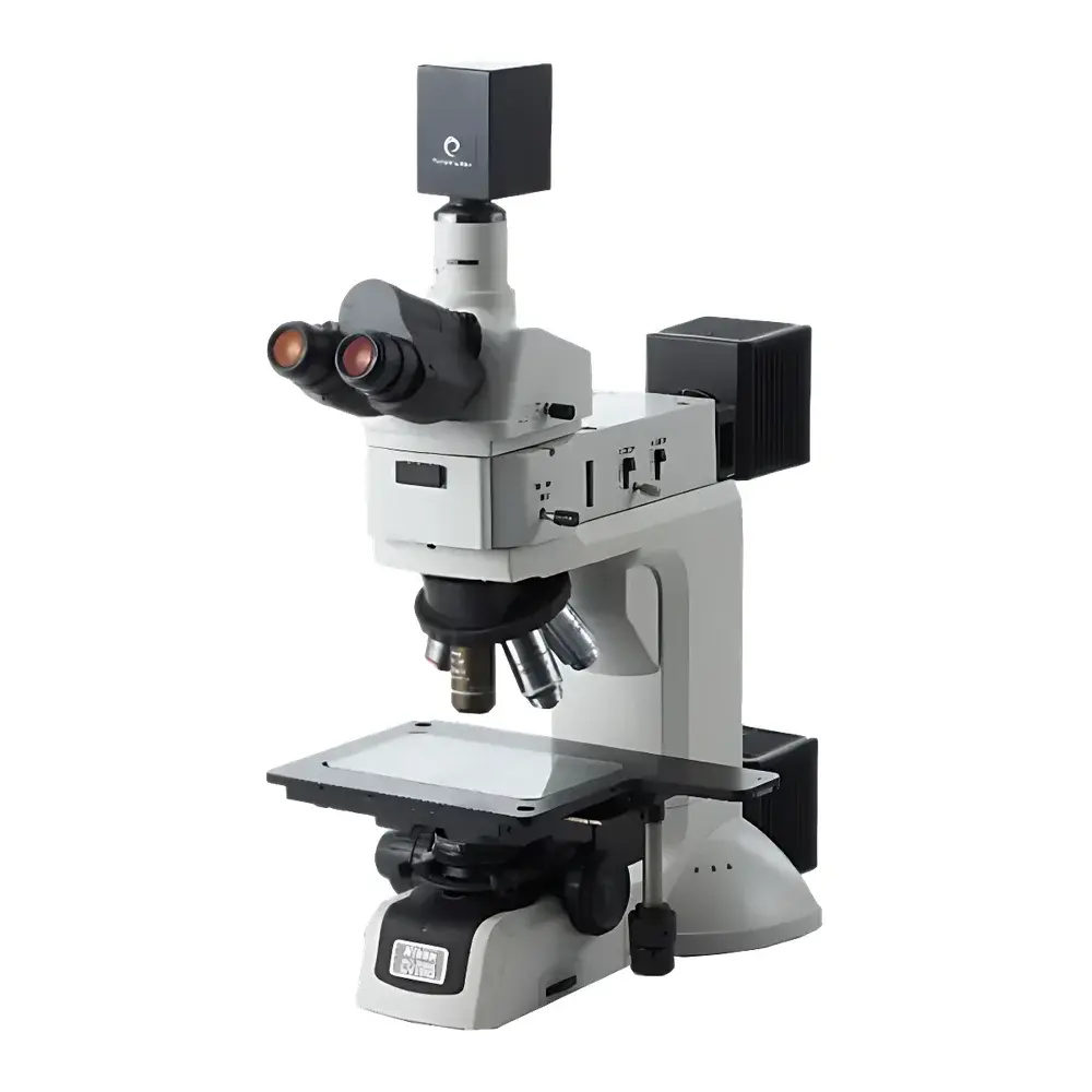
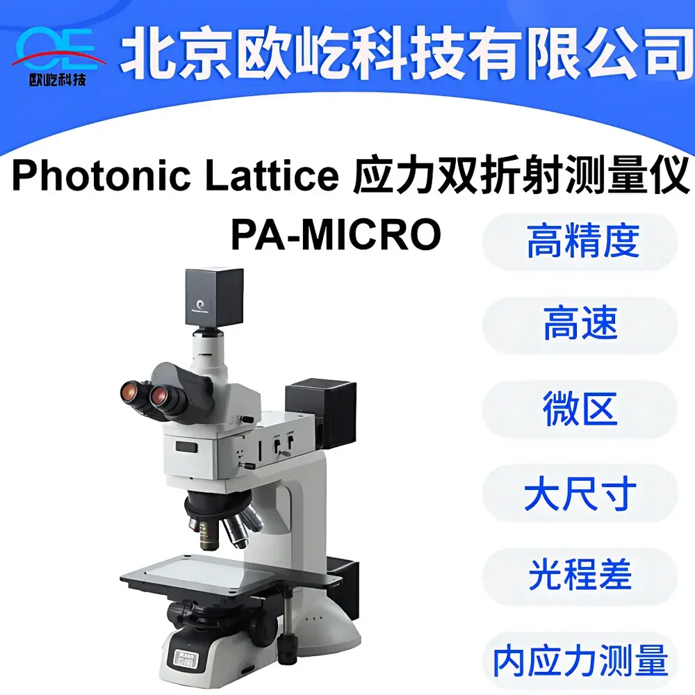
PHL PA-micro Microscopic Photoelastic Stress Analyzer
| Brand | Photonic Lattice |
|---|---|
| Origin | Japan |
| Model | PA-micro |
| Measurement Range | 0–130 nm |
| Repeatability | <1.0 nm |
| Pixel Resolution | 1120 × 868 |
| Wavelength | 520 nm |
| Objective Lenses | 5× (1.1 × 0.8 mm), 10× (0.5 × 0.4 mm), 20× (270 × 200 µm), 50× (110 × 80 µm), 100× (55 × 40 µm) |
| Dimensions | 250 × 487 × 690 mm |
| Weight | 11 kg |
| Interface | Gigabit Ethernet (camera signal) |
| Power Supply | AC 100–240 V, 50/60 Hz |
| Software | PA-View (for Micro) |
Overview
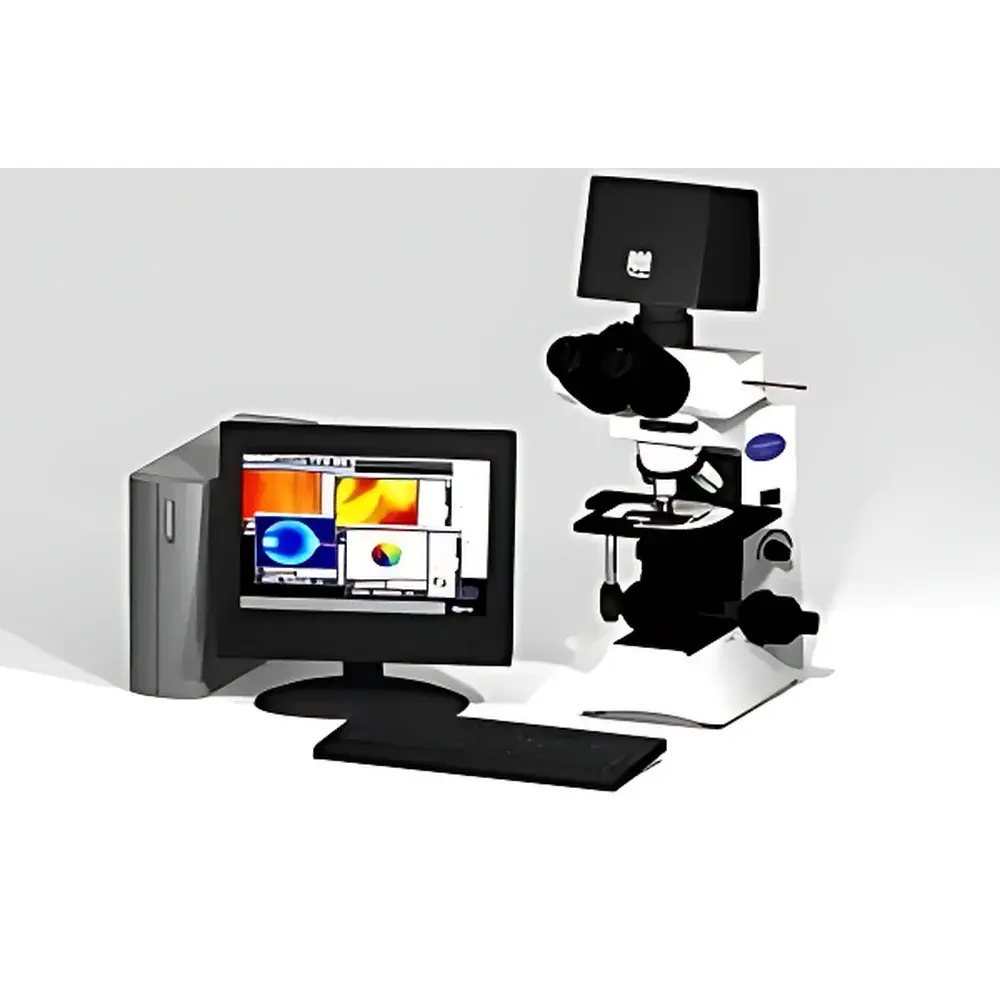
The PHL PA-micro Microscopic Photoelastic Stress Analyzer is a high-resolution, quantitative birefringence measurement system engineered for non-contact, full-field stress evaluation at the microscale. Based on the principle of polarization interference microscopy, the instrument measures retardation (phase difference Δδ) induced by internal mechanical stress in transparent and semi-transparent dielectric materials. By illuminating the sample with monochromatic linearly polarized light at 520 nm and analyzing the resulting elliptical polarization state through a calibrated analyzer and high-sensitivity CMOS camera, the PA-micro reconstructs spatially resolved retardation maps with sub-nanometer sensitivity. Its optical architecture integrates precision strain-optic calibration, temperature-stabilized illumination, and vibration-damped mechanical design—enabling stable, repeatable measurements under laboratory or controlled production-floor conditions. The system is particularly suited for characterizing residual stress, thermal stress, and processing-induced anisotropy in optically active materials where conventional mechanical testing is impractical.
Key Features
- Sub-nanometer repeatability (<1.0 nm) across full dynamic range (0–130 nm), validated per ISO 11146 and JIS Z 8766 standards for optical metrology.
- Five interchangeable high-numerical-aperture microscope objectives (5× to 100×), supporting field-of-view scalability from 1.1 × 0.8 mm down to 55 × 40 µm—enabling both macro-defect screening and localized stress profiling at wafer-edge or thin-film interface regions.
- Gigabit Ethernet interface ensures real-time image streaming and synchronized acquisition at full 1120 × 868 pixel resolution without frame drop, compatible with time-resolved stress monitoring protocols.
- Integrated 520 nm LED source with spectral stability better than ±0.5 nm over 8-hour operation, minimizing wavelength drift-related uncertainty in retardation quantification.
- Modular mechanical platform with rigid aluminum alloy chassis and passive damping mounts—designed to meet ISO 25178 surface vibration requirements for optical metrology systems.
Sample Compatibility & Compliance
The PA-micro accommodates flat, polished, or coated specimens up to 150 mm in diameter and 50 mm in thickness—including fused silica wafers, BK7 and SF10 optical lenses, tempered glass displays, PET and PC polymer films, sapphire substrates, and semiconductor-grade quartz crystals. Samples require no metallization or coating; measurement relies solely on intrinsic birefringence. The system supports compliance workflows aligned with ASTM C1357 (stress birefringence in optical glass), ISO 10110-5 (surface stress in optical elements), and JEDEC JESD22-A112 (thermal stress in packaged ICs). Data acquisition logs include timestamped metadata, operator ID, environmental temperature/humidity tags, and objective lens identification—facilitating GLP/GMP audit readiness and 21 CFR Part 11-compliant electronic records when paired with validated PA-View software configuration.
Software & Data Management
PA-View (for Micro) is a Windows-based application providing real-time retardation mapping, vector orientation analysis, line-profile extraction, and statistical reporting (mean, std dev, min/max, histogram). It supports batch processing of multi-objective datasets, ROI-based averaging, and export of calibrated TIFF stacks with embedded EXIF metadata (including wavelength, exposure time, gain, and calibration coefficients). Raw data files are stored in HDF5 format to ensure bit-perfect fidelity and long-term archival integrity. The software includes built-in validation tools for daily performance verification using NIST-traceable reference retarders (e.g., Berek-type compensators), and generates PDF reports compliant with ISO/IEC 17025 documentation requirements. Remote operation via TCP/IP is supported for integration into automated inspection lines.
Applications
- Residual stress mapping in precision optical components during polishing and annealing process development.
- Quality control of smartphone cover glass and automotive HUD waveguides for localized stress-induced depolarization.
- Failure analysis of bonded silicon-on-insulator (SOI) wafers and MEMS packaging interfaces.
- Quantitative assessment of cure-induced shrinkage stress in UV-curable acrylate coatings and dental composites.
- Thermo-mechanical stress evolution studies in laser-heated microstructures using synchronized thermal imaging and birefringence capture.
FAQ
What is the minimum measurable retardation step size?
The system achieves theoretical resolution of 0.1 nm under optimal SNR conditions; practical detection limit is defined by photon shot noise and is typically 0.3 nm RMS for 1-second integration at 520 nm.
Can the PA-micro measure stressed samples with anti-reflective coatings?
Yes—the instrument operates in transmission mode and is insensitive to single-layer AR coatings below 100 nm thickness; multilayer broadband coatings may require spectral correction routines available in PA-View.
Is calibration traceable to national standards?
Photonic Lattice provides factory calibration using NIST-traceable quarter-wave and half-wave retardation standards; annual recalibration services include uncertainty budget documentation per ISO/IEC 17025.
Does the system support custom scripting or API access?
PA-View exposes a COM interface and Python-compatible DLL library for automated measurement sequencing, third-party GUI integration, and inline SPC feedback loops.
What environmental conditions are recommended for optimal performance?
Ambient temperature stability of ±0.5 °C/hour and relative humidity between 30–60% RH are recommended; operation outside these ranges requires optional environmental enclosure add-ons.


