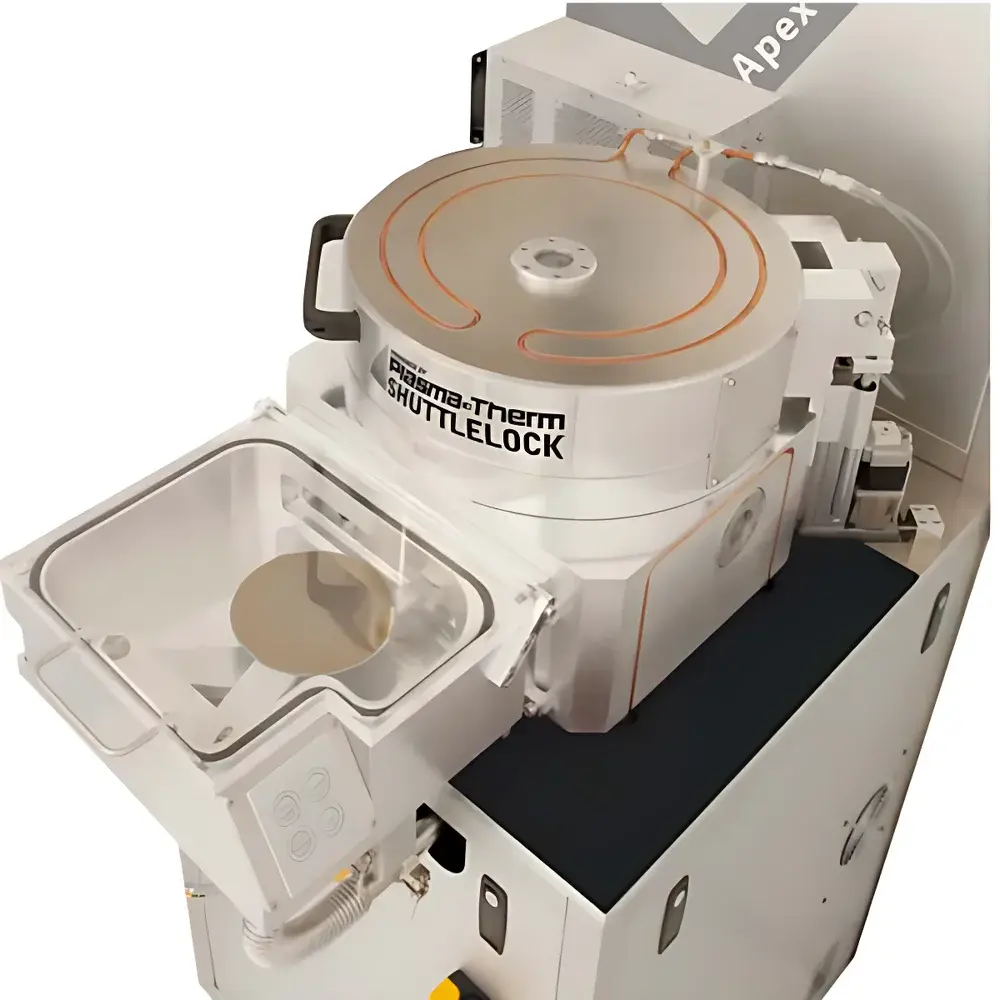
Plasma-Therm Takachi ICP Plasma Etching System
| Brand | Plasma-Therm |
|---|---|
| Origin | USA |
| Model | Takachi |
| Etch Principle | Inductively Coupled Plasma (ICP) |
| Etch Rate | SiO₂ ≥ 1500 Å/min |
| Selectivity | SiO₂ to Photoresist = 1.0–1.5:1 |
| Si₃N₄ to Photoresist = 1.0–1.2 | 1 |
| Uniformity | ≤ ±2% |
| Application Scope | Dielectrics (SiO₂, Si₃N₄, metal oxides), Polymers (photoresists, polyimides, BCB, SU-8), Semiconductors (Si, Ge, III–V compounds including GaAs, AlGaAs, GaN, InP), SiC |
Overview
The Plasma-Therm Takachi ICP Plasma Etching System is a high-precision, benchtop-compatible dry etch platform engineered for advanced semiconductor process development and nanoscale fabrication. Utilizing dual-frequency inductively coupled plasma (ICP) source technology, the system separates ion energy control (via bias RF) from plasma density generation (via ICP RF), enabling independent optimization of etch rate, anisotropy, selectivity, and sidewall profile control. This decoupling is critical for achieving sub-100 nm feature fidelity in R&D and low-volume production environments where process window robustness and repeatability are paramount. Designed and manufactured in the United States, the Takachi system integrates vacuum chamber architecture, precision gas delivery manifolds, and real-time endpoint detection capability—making it suitable for both reactive ion etching (RIE) and high-density plasma (HDP) regimes across silicon, compound semiconductors, and emerging wide-bandgap materials.
Key Features
- Dual-frequency RF architecture: 13.56 MHz ICP source for high-density plasma generation + independently controlled 13.56 MHz or 2 MHz bias RF for fine-tuned ion energy modulation
- Stainless-steel vacuum chamber with integrated ceramic-coated electrodes and water-cooled chuck for thermal stability during extended etch cycles
- Mass flow controllers (MFCs) for up to six process gases (e.g., CF₄, CHF₃, SF₆, O₂, Ar, Cl₂), supporting complex chemistries for dielectric, polymer, and III–V material etching
- Real-time optical emission spectroscopy (OES) endpoint detection with configurable spectral windows and threshold-based trigger logic
- Programmable recipe management with up to 99 user-defined processes, each supporting multi-step sequences with timed gas switching and power ramping
- Compliance-ready hardware architecture: supports optional audit trail logging, electronic signatures, and secure user role management for GLP/GMP-aligned workflows
Sample Compatibility & Compliance
The Takachi system accommodates wafers up to 200 mm (8-inch) diameter and supports standard cassette-to-chamber loading. Its process flexibility extends across diverse substrate classes: thermally grown and CVD-deposited SiO₂ and Si₃N₄; organic and inorganic photoresists (including deep-UV and e-beam resists); polyimide, BCB, and SU-8; elemental semiconductors (Si, Ge); compound semiconductors (GaAs, AlGaAs, InP, GaN); and wide-bandgap materials (SiC). All wetting parts are constructed from ultra-high-purity alumina and quartz to minimize metallic contamination. The system conforms to SEMI S2/S8 safety standards and meets CE marking requirements for electromagnetic compatibility (EMC) and low-voltage directive compliance. Optional IQ/OQ documentation packages are available to support qualification under ISO 9001, ISO/IEC 17025, and FDA 21 CFR Part 11–compliant environments.
Software & Data Management
Control is managed via Plasma-Therm’s proprietary EtchView™ software suite, running on a Windows-based industrial PC with deterministic real-time OS extensions. The interface provides full remote monitoring, live parameter visualization (RF forward/reflected power, chamber pressure, gas flows, temperature), and automated data logging compliant with ASTM E2651–21 for semiconductor process data integrity. All recipe executions generate timestamped, digitally signed log files containing setpoints, actuals, OES traces, and fault event records—enabling traceability for internal audits or regulatory submissions. Data export supports CSV, XML, and HDF5 formats; integration with MES platforms (e.g., FactoryTalk, CIM300) is supported via SECS/GEM protocol stack.
Applications
- Research & development of novel etch chemistries for high-k dielectrics and 2D materials
- Failure analysis (FA) sample preparation requiring damage-free cross-sectioning and trench isolation
- MEMS device release etching with high aspect-ratio control and minimal stiction
- Photonic integrated circuit (PIC) waveguide definition in Si, SiN, and InP platforms
- Nanopatterning for plasmonic structures and quantum dot arrays using hard mask transfer
- Pilot-line processing of GaN-on-Si HEMTs and SiC power devices with tight CD uniformity control
FAQ
What vacuum level does the Takachi system achieve prior to plasma ignition?
Base pressure is typically ≤ 5 × 10⁻⁷ Torr, achieved using a turbomolecular pump backed by a dry scroll pump.
Is endpoint detection limited to optical emission spectroscopy?
Standard configuration includes broadband OES; optional residual gas analyzer (RGA) integration is available for mass-spectrometry-based endpoint verification.
Can the system be upgraded for 300 mm wafer processing?
No—the Takachi is purpose-built for 150 mm and 200 mm substrates; Plasma-Therm offers the VERSA series for 300 mm applications.
Does the system support cryogenic etching for high-aspect-ratio silicon features?
Yes—optional liquid nitrogen cooling of the electrostatic chuck enables sub-−100°C etch temperatures for Bosch and cryo-RIE processes.
How is process reproducibility validated across tool installations?
Plasma-Therm provides standardized qualification wafers and reference etch protocols aligned with SEMI E10 and E142 standards for inter-tool correlation studies.


