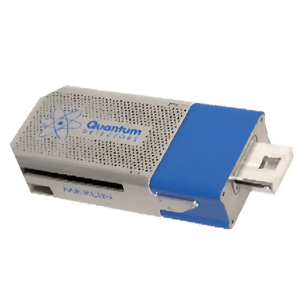
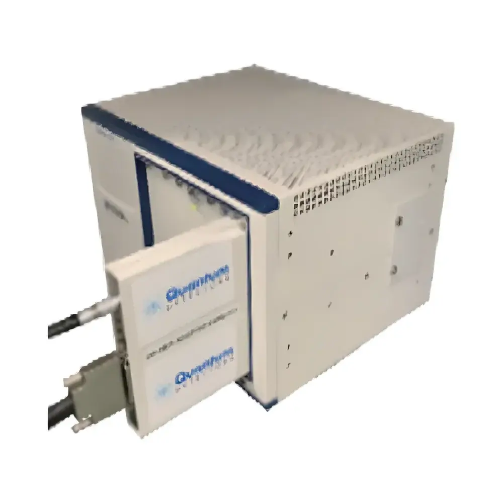
Quantum Detectors MerlinEM Direct Electron Detector for Transmission Electron Microscopy
| Brand | Quantum Detectors |
|---|---|
| Origin | United Kingdom |
| Manufacturer Type | Authorized Distributor |
| Origin Category | Imported |
| Model | MerlinEM |
| Pricing | Available Upon Request |
| Detector Material | 500 µm thick silicon |
| Detector Type | Reverse-biased hybrid silicon diode array |
| Pixel Size | 55 × 55 µm |
| Active Area | 1R (single chip): 14 × 14 mm² |
| 4R/4S (quad-chip) | 28 × 28 mm² |
| Pixel Count | 1R: 256 × 256 |
| 4R/4S | 512 × 512 |
| Readout Noise | Effectively 0 e⁻ (threshold-based discrimination) |
| Signal-to-Noise Ratio (SNR) | 107:1 |
| Detective Quantum Efficiency (DQE) at 60 keV | 1.0 (zero frequency), 0.45 (Nyquist frequency) |
| Modulation Transfer Function (MTF) at 60 keV | >0.62 at Nyquist frequency (mode-dependent) |
| Frame Rate (full-frame, continuous) | 18,800 fps (1-bit), 3,600 fps (6-bit), 1,800 fps (12-bit), 800 fps (24-bit) |
| Region-of-Interest (ROI) readout | up to 7,200 fps (128 × 256, 6-bit), 14,400 fps (64 × 256, 6-bit) |
| Inter-frame gap time | 0 µs |
| Dynamic Range | Up to 24-bit per pixel (16,777,216 counts/pixel) |
| Trigger Interface | 3.3 V / 5 V TTL pulse or software-controlled via TCP/IP |
| Energy Range | 30–300 keV |
| Software Suite | 4D STEM acquisition platform, LabVIEW drivers, GM3 integration interface, native TCP/IP communication |
| Mounting Options | Side-insertion retractable or bottom-fixed configuration |
| Optional Integration | NanoMEGAS precession electron diffraction (PED) interface |
Overview
The Quantum Detectors MerlinEM is a high-performance direct electron detector (DED) engineered specifically for advanced transmission electron microscopy (TEM) applications. Unlike scintillator-based indirect detectors, the MerlinEM employs a monolithic, reverse-biased silicon diode array to convert incident electrons directly into charge carriers within each pixel—eliminating light conversion losses and associated point-spread degradation. Its core architecture integrates custom application-specific integrated circuits (ASICs) with on-pixel threshold discrimination logic, enabling true single-electron event detection without readout noise. This zero-noise readout capability, combined with sub-microsecond frame intervals and fully programmable gain and bit-depth modes, positions the MerlinEM as a foundational tool for quantitative electron imaging, especially in dose-sensitive, dynamic, and low-dose regimes such as 4D scanning transmission electron microscopy (4D STEM), precession electron diffraction (PED), and time-resolved pump-probe experiments.
Key Features
- True Zero-Readout-Noise Detection: Each pixel incorporates dual-threshold discriminators that reject thermal and electronic noise below user-defined energy thresholds—ensuring no spurious counts are registered during acquisition.
- High DQE and MTF Performance: At 60 keV, the detector achieves DQE(0) = 1.0 and DQE(Nyquist) = 0.45, with MTF(Nyquist) > 0.62—meeting or exceeding the theoretical limits of ideal direct detection for structural analysis and phase contrast quantification.
- Ultra-High Dynamic Range: 24-bit counting depth per pixel (up to 16.7 million counts) enables simultaneous capture of weak diffraction spots and intense Bragg reflections within a single exposure—critical for crystallographic symmetry analysis and strain mapping.
- Sub-Millisecond Frame Rates & Zero Dead Time: Full-frame rates up to 18.8 kHz (1-bit mode) and ROI-accelerated acquisition support real-time beam tracking, drift correction, and multi-frame averaging without temporal gaps—minimizing specimen drift artifacts in long-duration acquisitions.
- Charge-Sharing Mitigation Architecture: On-chip inter-pixel communication allows neighboring pixels to jointly evaluate charge deposition events, reducing spatial blurring from charge diffusion and improving effective spatial resolution—particularly advantageous at lower accelerating voltages (e.g., 30–80 keV).
- Flexible Integration Pathways: Supports side-insertion retractable mounting for rapid exchange in double-tilt holders and bottom-fixed configurations compatible with high-tilt stages. Optional NanoMEGAS PED interface enables seamless synchronization of detector readout with goniometer motion and beam precession.
Sample Compatibility & Compliance
The MerlinEM is designed for use across a broad spectrum of TEM platforms—including JEOL, Thermo Fisher Scientific (FEI), and Hitachi systems—operating at accelerating voltages from 30 keV to 300 keV. Its radiation-hardened silicon sensor and robust ASIC design ensure long-term stability under prolonged electron irradiation, meeting requirements for GLP-compliant materials characterization workflows. While not certified to ISO/IEC 17025 or FDA 21 CFR Part 11 by default, the detector’s TCP/IP-native communication protocol and deterministic trigger timing support audit-ready data provenance when integrated into validated laboratory information management systems (LIMS) or TEM control suites compliant with GMP documentation standards.
Software & Data Management
The MerlinEM operates via a modular software ecosystem including native 4D STEM acquisition modules, LabVIEW-compatible drivers, and GM3-compatible interfaces for third-party microscope control. All data streams adhere to the open, metadata-rich EMD (Electron Microscopy Data) format, ensuring compatibility with widely adopted processing pipelines such as HyperSpy, PyXEM, and MRC2. Real-time streaming over Gigabit Ethernet enables on-the-fly frame filtering, region-of-interest binning, and histogram-based threshold adjustment—facilitating adaptive acquisition strategies without post-hoc reconstruction delays. Raw data files include embedded timestamps, hardware configuration logs, and detector calibration parameters, satisfying traceability requirements for peer-reviewed publication and regulatory submission.
Applications
- Quantitative 4D STEM for strain mapping, electric/magnetic field reconstruction, and differential phase contrast (DPC) imaging
- Precession electron diffraction (PED) and automated crystal orientation mapping (ACOM)
- Low-dose biological TEM, cryo-EM tilt-series acquisition, and beam-sensitive MOF/COF structural analysis
- Pump-probe electron microscopy experiments requiring precise synchronization between laser excitation and electron probe timing
- In situ TEM studies involving heating, biasing, or gas/liquid cells where high temporal resolution and signal fidelity are essential
- Nanobeam electron diffraction (NBED) and convergent beam electron diffraction (CBED) with single-shot pattern acquisition
FAQ
What is the minimum detectable electron energy threshold?
The MerlinEM supports electron energies down to 30 keV, enabled by its 500 µm thick high-resistivity silicon sensor and optimized backside illumination geometry.
Can the MerlinEM be used for cryo-EM applications?
Yes—the detector is compatible with standard cryo-transfer holders and has been validated for low-dose imaging of vitrified biological specimens at liquid nitrogen temperatures.
Does the system support hardware-triggered acquisition synchronized with external devices?
Yes—TTL-compatible trigger inputs (3.3 V / 5 V) allow precise synchronization with laser pulses, piezo stages, or fast deflectors, with jitter < 10 ns.
Is there a difference in performance between 1R and 4R configurations?
The 4R/4S quad-chip configuration doubles both active area and pixel count while maintaining identical per-pixel specifications; however, inter-chip alignment requires careful calibration for seamless mosaic stitching in wide-field diffraction applications.
How is calibration data managed and preserved across sessions?
Each acquisition embeds non-volatile calibration metadata—including gain maps, dark reference frames, and threshold offsets—ensuring reproducible quantitative intensity scaling across instruments and operators.


