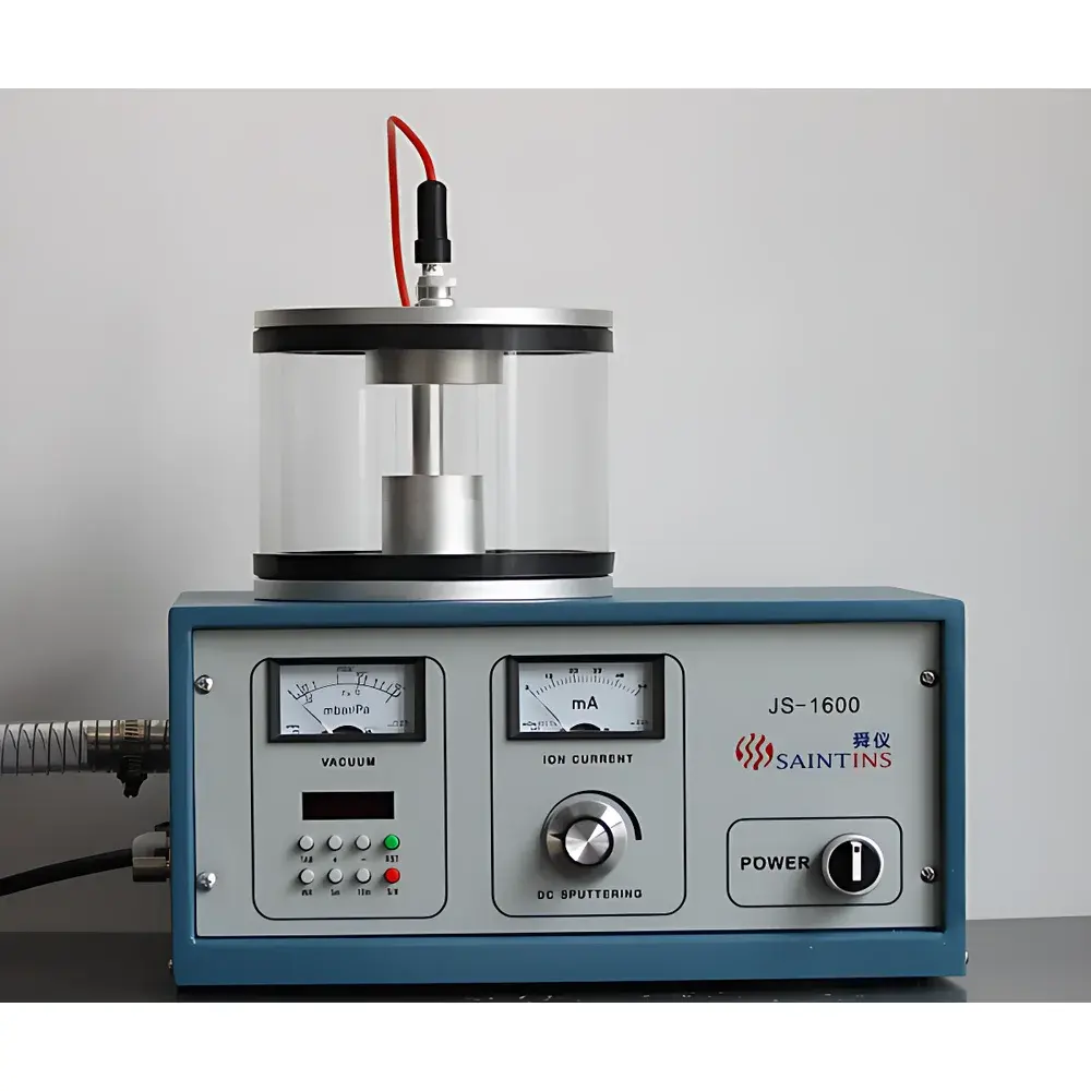
Saintins JS-1600 Compact DC Ion Sputter Coater
| Brand | Saintins |
|---|---|
| Origin | Jiangsu, China |
| Manufacturer Type | Direct Manufacturer |
| Country of Origin | China |
| Model | JS-1600 |
| Target Material | Gold (99.999% purity) |
| Target Diameter | 50 mm |
| Control Mode | Manual |
| Chamber Dimensions | Ø160 mm × H110 mm |
| Sample Stage Diameter | 50 mm |
| Sputtering Gas | Air or Argon |
| Vacuum Pump | VRD-4 rotary vane pump (1.1 L/s) |
| Operating Pressure Range | 1×10⁻¹–2×10⁻¹ mbar |
| Sputtering Voltage | –1600 V DC |
| Ion Current Range | 0–50 mA |
| Timer | Adjustable single-run duration |
| Gas Inlet | Precision needle valve with φ4×2.5 mm tubing port |
Overview
The Saintins JS-1600 Compact DC Ion Sputter Coater is a benchtop thin-film deposition system engineered for high-reproducibility conductive coating of non-conductive specimens prior to scanning electron microscopy (SEM) analysis. It operates on the principle of direct-current (DC) diode sputtering—where energetic ions generated in a low-pressure gas plasma (typically argon or ambient air) bombard a metallic target (cathode), ejecting atoms that subsequently condense as a uniform, nanoscale conductive layer onto grounded substrates placed on the anode (sample stage). This physical vapor deposition (PVD) process enables precise control over film thickness, morphology, and continuity—critical parameters for minimizing charging artifacts, enhancing secondary electron yield, and preserving surface topography during high-resolution SEM imaging. Designed for routine laboratory environments, the JS-1600 delivers robust performance without requiring ultra-high vacuum infrastructure or complex automation.
Key Features
- Compact Diode Architecture: Integrated two-electrode configuration with gold target (Ø50 mm, 0.1 mm thick, 99.999% purity) mounted as the upper cathode and a concentric sample stage (Ø50 mm) serving as the grounded anode—ensuring efficient plasma confinement and uniform ion flux distribution.
- Optimized Vacuum Chamber: Cylindrical stainless-steel chamber (Ø160 mm × 110 mm height) accommodates oversized or irregularly shaped samples while maintaining stable pressure dynamics across the operational range (1×10⁻¹–2×10⁻¹ mbar).
- Manual Precision Control: Independent adjustment of sputtering voltage (–1600 V DC), ion current (0–50 mA), and exposure time via analog dials and digital timer—enabling method development and fine-tuning for diverse material systems.
- Flexible Gas Handling: Equipped with a calibrated needle valve inlet compatible with φ4×2.5 mm flexible tubing; supports controlled introduction of argon (recommended for optimal film quality) or filtered ambient air (for rapid, cost-effective coating).
- Dedicated Vacuum System: Paired with a VRD-4 rotary vane pump (1.1 L/s pumping speed) capable of achieving base pressures suitable for stable glow discharge initiation and sustained sputtering without oil backstreaming contamination.
Sample Compatibility & Compliance
The JS-1600 accommodates a broad spectrum of non-conductive or semi-conductive specimens—including biological tissues, polymers, ceramics, geological sections, and insulating composites—without requiring pre-treatment or conductive adhesives. Its Ø50 mm sample stage permits standard SEM stub mounting (e.g., aluminum or copper stubs with carbon tape), while the large chamber volume allows simultaneous coating of multiple small samples or extended-area substrates (e.g., TEM grids, sensor wafers). The system complies with general laboratory safety standards for low-voltage DC operation and sealed vacuum systems. While not certified to ISO/IEC 17025 or GLP/GMP out-of-the-box, its manual controls and repeatable process parameters support traceable method documentation required for internal QA/QC protocols and academic reproducibility reporting.
Software & Data Management
The JS-1600 operates via fully manual interface—no embedded software or digital data logging is included. All operational parameters (voltage, current, time, gas flow estimate) must be recorded externally by the user. This architecture ensures long-term reliability, eliminates firmware obsolescence risks, and aligns with laboratories prioritizing audit-ready procedural transparency. Users may integrate external data acquisition tools (e.g., USB multimeters, stopwatch apps, or LIMS-compatible spreadsheets) to maintain full experimental metadata—supporting compliance with ISO 13847, ASTM E1558, and USP guidelines for SEM sample preparation validation.
Applications
- Routine metallization of biological specimens (e.g., plant epidermis, insect cuticle, freeze-fractured membranes) for high-contrast, low-charging SEM imaging.
- Preparation of insulating thin-film devices (e.g., perovskite layers, MOFs, aerogels) for cross-sectional analysis and elemental mapping (EDS).
- Fabrication of reference electrodes on polymer substrates for electrochemical characterization.
- Deposition of conductive seed layers on microfluidic chips or MEMS components prior to FIB-SEM tomography.
- Teaching labs: Demonstrating fundamental principles of plasma physics, thin-film growth kinetics, and surface modification techniques.
FAQ
What target materials are compatible with the JS-1600?
The system is configured for gold sputtering by default, but the target holder accepts custom discs (Ø50 mm, ≤0.2 mm thickness) made from Pt, Ag, Au/Pd, Cr, or Ir—subject to DC conductivity and thermal stability under –1600 V bias.
Can argon gas be substituted with nitrogen or oxygen?
No. Reactive gases such as O₂ or N₂ may oxidize or nitride the target surface, destabilize the plasma, and compromise film adhesion and conductivity. Only inert gases (Ar) or filtered dry air are recommended.
Is vacuum oil contamination a concern with the VRD-4 pump?
The VRD-4 is a single-stage rotary vane pump with integrated exhaust filtration; when operated within its specified duty cycle (<30 min continuous sputtering), oil backstreaming into the chamber remains negligible for routine SEM prep applications.
How is film thickness estimated without real-time monitoring?
Thickness is inferred empirically using standardized calibration curves correlating sputtering time, current, and pressure—established via profilometry or TEM cross-sectioning on reference samples. Typical gold films range from 2–10 nm after 30–120 s at 30 mA.
Does the JS-1600 meet FDA 21 CFR Part 11 requirements?
No. As a manually operated instrument without electronic audit trails, user authentication, or data integrity safeguards, it does not satisfy Part 11 criteria—but remains suitable for research, education, and non-regulated QC environments.


