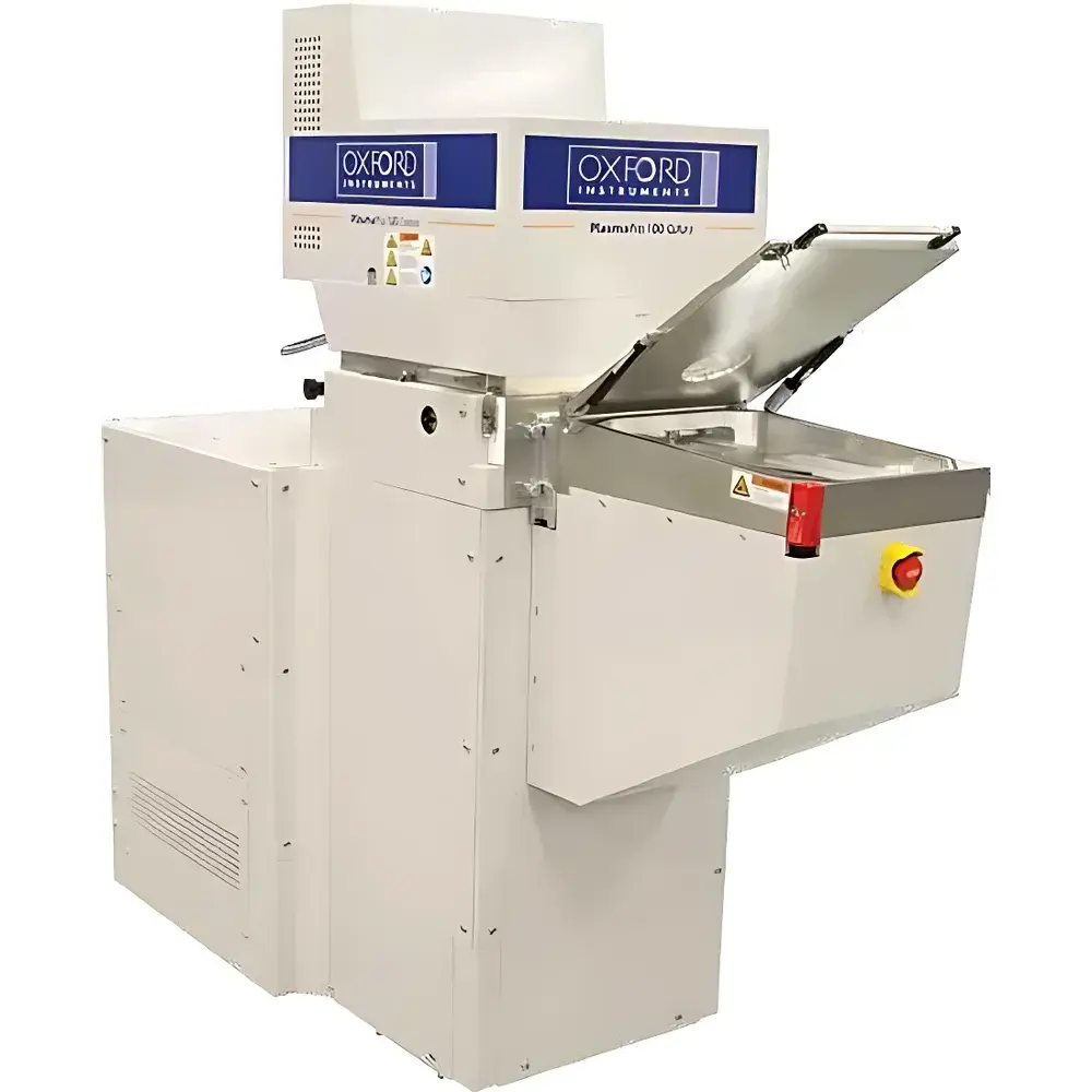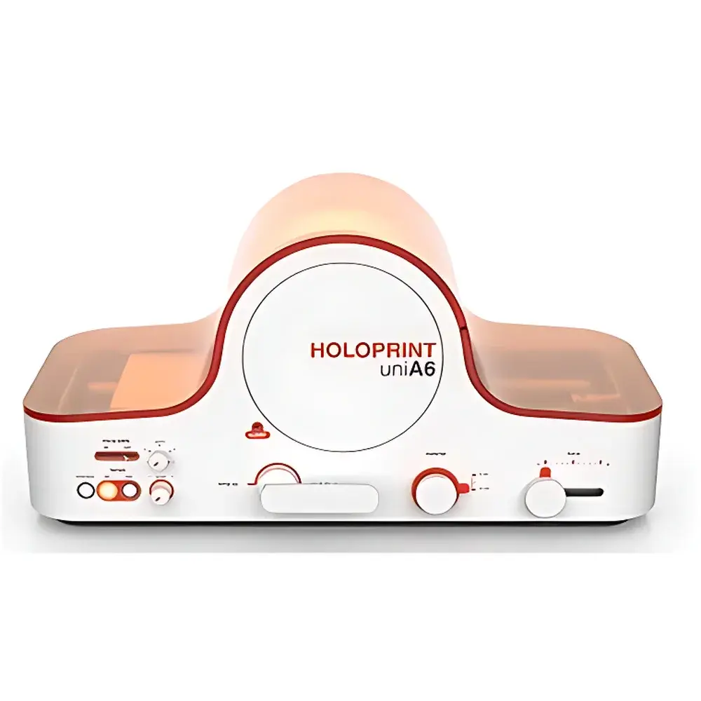
Stensborg HoloPrinter R2P Nanoimprint System
| Brand | Stensborg |
|---|---|
| Origin | Denmark |
| Model | HoloPrinter |
| Minimum Feature Size | 2 µm |
| Electron Beam Diameter | 1 µm |
| Accelerating Voltage Range | 30 kV |
Overview
The Stensborg HoloPrinter R2P Nanoimprint System is a roll-to-plate (R2P) nanoscale patterning platform engineered for high-throughput, high-fidelity replication of micro- and nanostructured optical surfaces. Unlike conventional electron beam lithography systems that operate in vacuum-based serial writing mode, the HoloPrinter integrates direct-write electron beam exposure with continuous or step-and-repeat nanoimprint processing—enabling rapid, scalable fabrication of sub-micron 3D topographies on flexible or rigid substrates. Its core architecture leverages a focused 1 µm electron beam at 30 kV acceleration voltage to expose resist-coated webs or plates, followed by precise thermal or UV-curable imprint transfer using master templates. This hybrid approach bridges the gap between maskless nanofabrication and industrial roll-based manufacturing, delivering structural fidelity down to 2 µm minimum feature size without requiring pre-fabricated foils or complex alignment infrastructure.
Key Features
- Roll-to-plate (R2P) configuration optimized for lab-scale prototyping and pilot-line production of optical security elements and functional microstructures
- Integrated 30 kV electron beam column with ≤1 µm spot size for high-resolution resist exposure on pre-coated substrates
- Modular template handling system supporting both rigid quartz masters and flexible nickel shims for multi-cycle imprint durability
- Real-time web tension control and precision stage synchronization to ensure <±100 nm overlay accuracy across A6-format (105 × 148 mm) imprint areas
- Thermal and UV-curable imprint modes compatible with industry-standard nanoimprint resists (e.g., OrmoStamp®, NOA81, and proprietary Stensborg formulations)
- Compact desktop footprint (UNI A6 DT form factor) designed for integration into cleanroom environments with Class 1000 or better air classification
Sample Compatibility & Compliance
The HoloPrinter accommodates a broad range of substrate formats including PET, PC, PMMA, silicon wafers (up to 100 mm), and pre-coated polymer films. It supports both solvent-based and solvent-free resist chemistries, enabling compatibility with ISO 12224-2 (holographic security features), ISO/IEC 14443 (RFID tag embossing), and ASTM D3359 (adhesion testing) workflows. All motion control firmware and exposure sequencing modules comply with IEC 61508 SIL2 functional safety requirements. Data logging and user access protocols meet GLP audit trail standards per FDA 21 CFR Part 11 when configured with optional electronic signature modules.
Software & Data Management
Operation is managed via Stensborg’s proprietary HoloControl Suite—a Windows-based application supporting G-code and DXF import, dose calibration mapping, and real-time beam current monitoring. The software includes built-in pattern stitching algorithms for seamless tiling across >100 mm² areas and automated focus compensation routines for non-planar substrates. Exported process logs include timestamped exposure parameters, stage position history, and environmental sensor data (temperature, humidity, vacuum level). Raw metrology files (e.g., AFM height maps, SEM cross-sections) can be linked to specific imprint batches for traceability in quality-controlled environments.
Applications
- High-security holographic labels for banknotes, pharmaceutical packaging, and ID documents
- Mass-producible metasurfaces for augmented reality waveguide coupling and directional backlighting
- Nanostructured anti-reflective and light-trapping coatings for photovoltaic modules and OLED displays
- Microfluidic channel replication with aspect ratios >5:1 for point-of-care diagnostic cartridges
- Replication of diffractive optical elements (DOEs) for laser beam shaping and LiDAR illumination optics
- Research-grade fabrication of plasmonic lattices and photonic crystal slabs for academic and industrial photonics labs
FAQ
Is the HoloPrinter compatible with standard semiconductor cleanroom protocols?
Yes—it operates under ambient or low-vacuum conditions and meets SEMI S2/S8 safety guidelines; no dedicated high-vacuum infrastructure is required.
Can it produce features below 200 nm?
While the specified minimum line width is 2 µm for full-field R2P throughput, sub-200 nm features are achievable via localized e-beam exposure on static plates using optional high-resolution deflection modes.
Does Stensborg provide master template design and fabrication support?
Yes—Stensborg offers end-to-end services including optical design consultation, binary and grayscale mask fabrication, and lifetime template maintenance under extended service agreements.
What resist thickness ranges are supported?
From 50 nm to 5 µm, depending on imprint mode (thermal vs. UV) and substrate thermal expansion coefficient.
Is remote diagnostics and software update capability available?
All units ship with embedded Ethernet connectivity and TLS-secured remote access for firmware updates and predictive maintenance analytics.
Related Products