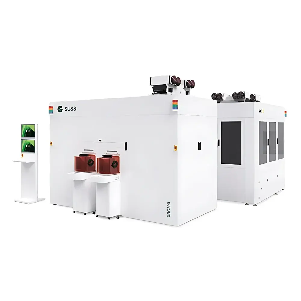
SUSS XBC300 Gen2 D2W/W2W Hybrid Bonding Platform
| Brand | SUSS MicroTec |
|---|---|
| Origin | Germany |
| Model | XBC300 Gen2 D2W/W2W |
| Substrate Compatibility | 200 mm to 300 mm wafers & tape-frame-mounted dies |
| Alignment Accuracy (W2W) | < 100 nm |
| Alignment Accuracy (D2W) | ±100 nm |
| Bonding Force | up to 300 N |
| Void Detection Resolution | > 500 µm (IR-based) |
| Minimum Die Pitch | 40 µm |
| Cleaning Chemistry Support | Dilute NH₄OH, citric acid, SC1-based organic removal |
| Process Environment | Cleanroom-compatible, modular cluster architecture |
Overview
The SUSS XBC300 Gen2 D2W/W2W Hybrid Bonding Platform is a fully integrated, cluster-tool architecture system engineered for advanced 3D semiconductor integration. It implements hybrid bonding—defined by simultaneous covalent oxide bonding and metal-to-metal interconnection—at wafer-level (W2W) and die-level (D2W), including both collective and sequential die placement configurations. The platform leverages electrostatic and thermocompression bonding mechanisms under ultra-high vacuum or controlled inert atmosphere, enabling atomic-scale interface formation with sub-100 nm overlay control. Designed in collaboration with SET Corporation SA, it serves R&D laboratories, pilot lines, and high-mix low-volume production environments where process flexibility, metrology traceability, and technology scalability are critical for next-generation heterogeneous integration—from SoC stacking to memory-on-logic architectures.
Key Features
- Multi-mode bonding capability: native support for W2W, collective D2W, and serial D2W within a single platform via interchangeable process modules.
- Sub-100 nm alignment accuracy for W2W using SUSS’ Inter-Substrate Alignment (ISA) technology, integrating optical fiducial referencing, global thermal calibration, and real-time distortion compensation across transparent and opaque substrates.
- ±100 nm die placement accuracy for D2W enabled by SET’s NEO HB die bonder module, featuring high-resolution vision metrology, active tip-tilt correction, and force-controlled touchdown with closed-loop pressure regulation up to 300 N.
- On-platform metrology station with full-field infrared (IR) imaging for in-situ alignment verification and void detection; capable of identifying interfacial voids larger than 500 µm with quantitative contrast analysis.
- Modular cleaning station supporting aqueous-based chemistries—including diluted NH₄OH, citric acid, and SC1 formulations—for particle removal and surface activation on both full wafers and tape-frame-mounted dies.
- Flexible substrate handling: accommodates 200 mm and 300 mm silicon and glass wafers, as well as tape frames with standard EIA-481 compliant carriers.
Sample Compatibility & Compliance
The XBC300 Gen2 D2W/W2W supports industry-standard semiconductor substrates including Si, SiO₂-coated Si, fused silica, and low-thermal-expansion glass (e.g., Borofloat®). Its process chamber design complies with SEMI S2/S8 safety standards and integrates particulate filtration meeting ISO Class 3 (Class 10) cleanroom requirements. All bonding recipes are configurable per lot and traceable via electronic log files compliant with FDA 21 CFR Part 11 for audit-ready documentation. The platform supports GLP/GMP-aligned process qualification protocols—including PQ, IQ, OQ—and is compatible with ASTM F3259 (Standard Guide for Hybrid Bonding Process Characterization) and JEDEC JEP197.1 (3D IC Interface Reliability Testing).
Software & Data Management
Controlled by SUSS’ proprietary BONDmaster™ software suite, the system provides recipe-driven operation with hierarchical parameter management, multi-user role-based access control, and real-time fault logging. All alignment data, bond force profiles, temperature ramp logs, and IR metrology images are timestamped and stored in an SQL-based database with automated backup. Data export conforms to SECS/GEM protocol for factory automation integration (e.g., MES, APC systems). Audit trails include operator ID, timestamp, parameter changes, and equipment state transitions—fully aligned with 21 CFR Part 11 electronic signature and record retention requirements.
Applications
- Development and transfer of hybrid bonding processes for HBM3 and future HBM generations requiring <10 µm microbump pitch and direct Cu-Cu interconnects.
- R&D of heterogeneous integration platforms combining logic, memory, and photonics on shared interposers or TSV-enabled substrates.
- Qualification of low-k dielectric bonding interfaces and plasma-activated surface preparation methods under controlled humidity and oxygen partial pressure.
- Process window characterization for thermal budget optimization—enabling bonding at ≤200 °C while maintaining interface strength >200 MPa after aging.
- Yield learning for D2W integration of compound semiconductor dies (e.g., GaN, SiC) onto silicon carrier wafers with minimal warpage-induced misalignment.
FAQ
What substrate sizes does the XBC300 Gen2 D2W/W2W support?
It handles 200 mm and 300 mm wafers, as well as tape-frame-mounted dies conforming to standard JEDEC packaging formats.
Is the system qualified for use in GMP-compliant pilot production?
Yes—the platform includes full electronic record and signature functionality, configurable audit trails, and validation documentation packages supporting IQ/OQ/PQ execution per ISO 9001 and IATF 16949 frameworks.
Can the IR metrology module detect sub-micron interfacial defects?
No—it is optimized for macro-void detection (>500 µm); sub-micron defect analysis requires complementary ex-situ techniques such as cross-sectional TEM or acoustic microscopy.
Does the system support low-temperature bonding for temperature-sensitive devices?
Yes—bonding can be performed between 150 °C and 350 °C, with process recipes validated down to 150 °C for MEMS and OLED-integrated stacks.
How is alignment verified during W2W bonding?
Through real-time ISA feedback using embedded optical reference marks and dynamic distortion mapping, with post-bond overlay measured via automated IR image correlation.
Related Products


