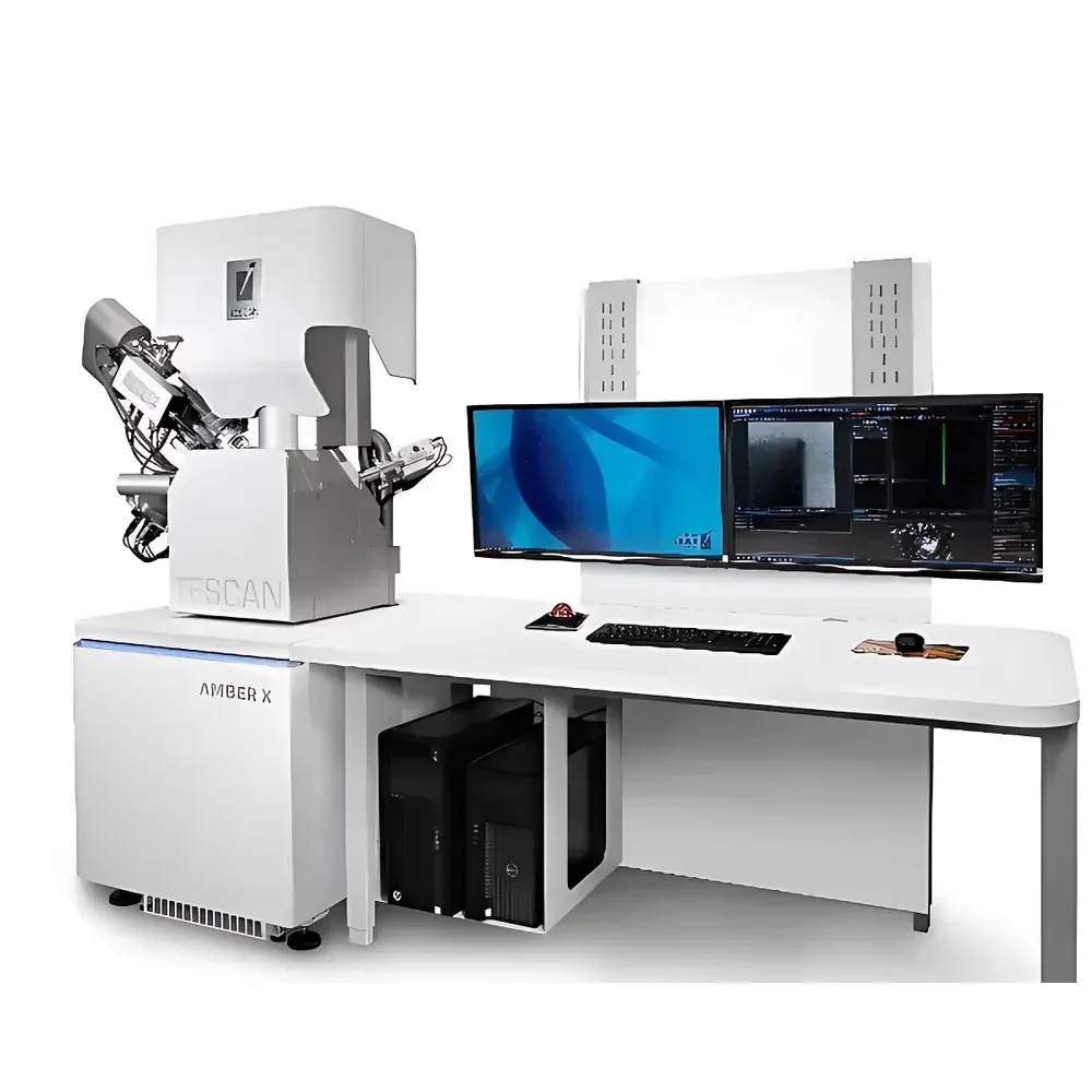
TESCAN AMBER X Xenon Plasma Focused Ion Beam–Scanning Electron Microscope
| Brand | TESCAN |
|---|---|
| Origin | Czech Republic |
| Model | TESCAN AMBER X |
| Ion Source | Xe Plasma FIB |
| Electron Source | Ultra-High-Resolution Schottky Field Emission Gun (FEG) |
| Maximum FIB Current | 1 µA |
| FIB Resolution | < 15 nm @ 30 kV |
| SEM Resolution | 1.5 nm @ 1 kV |
| Max Cross-Section Width | 1 mm |
| Cross-Section Preparation Time | ≤ 3.5 h |
Overview
The TESCAN AMBER X is an integrated dual-beam platform combining a xenon plasma focused ion beam (Xe Plasma FIB) with an ultra-high-resolution, magnetic field-free scanning electron microscope (UHR FEG-SEM). Engineered for precision materials science workflows, it enables simultaneous high-throughput nanofabrication, artifact-minimized sample preparation, and multi-modal structural and compositional characterization—without the deleterious effects associated with gallium ion implantation. Unlike conventional Ga⁺ FIB systems, the AMBER X leverages xenon’s chemical inertness and high sputter yield to deliver clean, contamination-free milling of sensitive materials—including aluminum alloys, battery cathodes, soft polymers, and TEM lamellae—while preserving native microstructure, crystallographic integrity, and mechanical properties. Its field-free SEM column ensures unimpeded operation of magnetic or beam-sensitive detectors (e.g., EBSD, in-lens STEM), making it uniquely suited for correlative microscopy where quantitative phase mapping, strain analysis, and orientation imaging must coexist with high-fidelity ion milling.
Key Features
- Xenon plasma FIB source delivering up to 1 µA total ion current, enabling rapid large-area milling (up to 1 mm wide cross-sections) with sub-15 nm feature resolution at 30 kV.
- BrightBeam™ UHR SEM column featuring a cold-field emission gun, optimized electromagnetic lens design, and zero-residual magnetic field—guaranteeing distortion-free imaging of ferromagnetic, superconducting, and magnetically labeled specimens.
- Piezo-driven aperture changer for dynamic, millisecond-scale switching between high-current milling and high-resolution imaging modes without mechanical hysteresis.
- Integrated tilt-and-rotate sample stage with real-time secondary electron monitoring during cross-section polishing—effectively suppressing curtaining artifacts and enabling in situ quality assessment.
- Enhanced detector architecture including in-column SE/BSE detectors, retractable EDS, and direct electron detection for low-dose STEM-in-SEM, all synchronized with FIB layer removal for true 3D correlative tomography.
Sample Compatibility & Compliance
The AMBER X supports diverse material classes—from conductive metals and semiconductors to insulating ceramics, biological composites, and energy storage electrodes—without mandatory conductive coating in most cases, thanks to its low-voltage (<1 kV) high-resolution imaging capability and beam-induced charge compensation. It complies with ISO/IEC 17025 requirements for analytical instrument validation and supports audit-ready documentation per GLP and GMP frameworks. All software operations—including parameter logging, user access control, and session history—are traceable and exportable in formats compatible with FDA 21 CFR Part 11–compliant laboratory information management systems (LIMS). The system is routinely deployed in accredited failure analysis labs, semiconductor R&D centers, and advanced battery development facilities where metrological traceability and process reproducibility are mandated.
Software & Data Management
Controlled by TESCAN’s Essence™ platform, the AMBER X provides a modular, scriptable interface built on Python 3.9 with native support for Jupyter Notebook integration. Automated workflows—including cross-section generation, serial sectioning, and multi-detector synchronized acquisition—are programmable via the TESCAN Automation Framework (TAF). All image, spectrum, and stage position metadata are stored in vendor-agnostic HDF5 containers compliant with the open NeXus standard. Raw data export supports TIFF, MRC, and EMDB-compatible formats for third-party reconstruction (e.g., Avizo, Dragonfly, TomoJ). Audit trails record every user action, instrument state change, and calibration event with UTC timestamps and digital signatures—ensuring full compliance with ISO 9001, ASTM E2865, and IEC 61508 functional safety guidelines.
Applications
- Rapid preparation of >1 mm-wide cross-sections for metallurgical interface analysis, interconnect inspection, and solder joint reliability assessment—with sub-micron surface roughness after plasma-FIB polishing.
- High-fidelity 3D FIB-SEM tomography of porous media, composite reinforcements, and electrode microstructures, accelerated by adaptive layer-thickness optimization and real-time drift correction.
- EBSD-based crystallographic tomography: seamless integration of static EBSD pattern indexing with sequential FIB slicing enables grain boundary network reconstruction and local misorientation mapping in polycrystalline systems.
- Ga-free TEM lamella fabrication from beam-sensitive organic-inorganic hybrid perovskites and lithium metal anodes—preserving redox states and interfacial chemistry for subsequent cryo-TEM or APT analysis.
- In situ nanomechanical testing: site-specific milling of micro-cantilevers or MEMS structures followed by nanoindentation or tensile testing inside the chamber using integrated micromanipulators.
FAQ
How does xenon plasma FIB differ from traditional gallium FIB in terms of sample damage?
Xenon ions do not chemically react with or implant into most materials, eliminating lattice disorder, amorphization, and elemental redistribution commonly induced by Ga⁺ bombardment—particularly critical for Al, Mg, Li-based compounds, and oxide heterostructures.
Can the AMBER X perform automated serial sectioning for 3D reconstruction?
Yes. Its embedded tomography module coordinates FIB slicing, stage repositioning, and multi-detector acquisition (SE, BSE, EDS, EBSD) with sub-5 nm Z-step accuracy and automated drift compensation across >1000 layers.
Is magnetic field-free operation essential for EBSD analysis?
Absolutely. Residual magnetic fields from conventional SEM columns deflect backscattered electrons, degrading Kikuchi pattern fidelity and indexing confidence; the AMBER X’s zero-field column ensures optimal pattern sharpness and angular resolution down to 0.05°.
What level of automation is supported for cross-section preparation?
Fully automated workflows—from initial fiducial placement and trench milling to final polishing and endpoint detection via real-time SE signal thresholding—are configurable and repeatable across users and sessions.
Does the system support remote operation and data sharing in collaborative environments?
Yes. Essence™ includes secure web-based remote desktop access, role-based data sharing portals, and API endpoints for integration with institutional HPC clusters and cloud-based visualization platforms.


