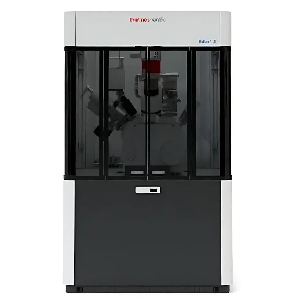
Thermo Fisher Scientific Helios 5 DualBeam Focused Ion Beam-Scanning Electron Microscope
| Brand | Thermo Fisher Scientific |
|---|---|
| Origin | Czech Republic |
| Model | Helios 5 DualBeam |
| Landing Voltage Range | 20 eV – 30 keV |
| SEM Resolution | Down to 0.6 nm @ 15–30 keV (depending on configuration) |
| FIB Current Range | 1 pA – 100 nA |
| Ion Acceleration Voltage | 500 V – 30 kV |
| Stage Travel | Up to 150 × 150 × 10 mm (X/Y/Z, model-dependent) |
| Automated TEM Lamella Preparation | Supported (via AutoTEM 5 software) |
| STEM Imaging Capability | Integrated (sub-nm resolution at 30 keV) |
| Compliance | Designed for GLP/GMP environments |
Overview
The Thermo Fisher Scientific Helios 5 DualBeam is a high-performance focused ion beam–scanning electron microscope (FIB-SEM) engineered for nanoscale imaging, precision sample preparation, and correlative 3D characterization in advanced materials science, semiconductor R&D, and life sciences applications. Built upon the proven Elstar electron optical platform and Tomahawk HT or Phoenix ion column architectures, the system integrates a high-brightness Schottky field emission gun (FEG), magnetic immersion objective lens, and dual-beam coaxial alignment to deliver sub-nanometer spatial resolution in both SEM and STEM modes. Its core functionality centers on simultaneous or sequential electron beam imaging and gallium ion beam milling—enabling site-specific cross-sectioning, TEM lamella extraction, atom probe tomography (APT) specimen preparation, and serial sectioning for 3D electron tomography. The instrument operates under ultra-high vacuum conditions with multi-stage differential pumping, ensuring stable beam performance and minimal contamination during extended automated runs.
Key Features
- Coaxial DualBeam architecture with real-time beam overlap verification and drift-compensated navigation for sub-10 nm targeting accuracy.
- FLASH (Fast Lens Alignment & Stigmation Handling) technology—automates astigmatism correction, beam centering, and focus optimization via single-click interface interaction, reducing image optimization time by up to 90%.
- Elstar high-resolution SEM column featuring a high-stability Schottky FEG, enabling consistent analytical current delivery from 0.8 pA to 176 nA across 200 V–30 kV acceleration range.
- Tomahawk HT or Phoenix ion columns offering wide current range (1 pA–100 nA), low-voltage ion imaging (1,000 h).
- Five-axis motorized stage with piezo-driven XYR axes (up to 150 mm X/Y travel, ±90° tilt, 360° continuous rotation) and precise eucentric height control for reproducible lamella positioning.
- Integrated detectors including in-column TLD-SE/BSE, retractable DBS (Divided Backscatter Detector), STEM 3+ segmented detector, and Nav-Cam navigation camera for rapid sample survey and feature localization.
Sample Compatibility & Compliance
The Helios 5 DualBeam accommodates a broad spectrum of conductive and non-conductive specimens—including bulk metals, ceramics, polymers, geological samples, and biological tissues (with appropriate coating or charge compensation). Sample dimensions support diameters up to 150 mm and heights up to 85 mm, with maximum mass handling of 5 kg at 0° tilt. All configurations meet ISO 14644-1 Class 5 cleanroom compatibility standards for semiconductor lab integration. The system’s firmware and AutoTEM 5 software are architected to comply with regulatory data integrity requirements: full electronic audit trails, user access controls, and secure data export protocols align with FDA 21 CFR Part 11, EU Annex 11, and GLP/GMP documentation frameworks. Routine maintenance logs, calibration records, and session metadata are timestamped and cryptographically signed to support laboratory accreditation audits.
Software & Data Management
AutoTEM 5 serves as the unified workflow engine for automated lamella preparation, serial sectioning, and correlative analysis. It provides scriptable protocol templates, machine-learning-assisted feature recognition (e.g., grain boundaries, interfaces, defects), and real-time process monitoring with adaptive endpoint detection. All acquired images, stage coordinates, beam parameters, and log files are stored in a vendor-neutral, metadata-rich format compliant with the EMDB/EMPIAR data deposition standards. Raw data export supports TIFF, MRC, and HDF5 containers with embedded calibration headers. Remote operation is enabled via secure TLS-encrypted client-server architecture, allowing off-site monitoring and intervention without compromising local network security policies.
Applications
- Transmission electron microscopy (TEM) specimen preparation: Site-specific lift-out of electron-transparent lamellae (down to 7 nm final thickness) with minimal curtaining and amorphous layer formation.
- Atom probe tomography (APT) tip fabrication: High-fidelity needle-shaped specimen generation with controlled apex radius and crystallographic orientation preservation.
- 3D microstructure reconstruction: Serial FIB-SEM tomography of battery cathodes, turbine alloys, and composite interfaces at isotropic voxel resolutions <10 nm.
- Semiconductor failure analysis: Cross-sectional imaging of BEOL interconnects, gate stacks, and embedded memory cells with voltage contrast and EBIC capability.
- In situ nanomechanical testing: Integration with nanoindenter stages for real-time observation of dislocation dynamics, crack propagation, and phase transformation under load.
FAQ
What vacuum level does the Helios 5 DualBeam maintain during operation?
The system employs a multi-stage differential pumping scheme to sustain base pressures below 1 × 10⁻⁷ mbar in the electron column and 5 × 10⁻⁶ mbar in the ion column during active milling—critical for minimizing Ga⁺ redeposition and beam-induced contamination.
Is the Helios 5 compatible with third-party TEM holders and transfer systems?
Yes—the instrument supports standard Gatan, FEI, and Protochips TEM holder interfaces via its automated insertion/extraction module, enabling seamless transfer to JEOL, Thermo Fisher, or Hitachi TEM platforms.
How is beam alignment validated and maintained over time?
Daily automated alignment routines verify beam coincidence within ±5 nm tolerance using reference patterns and beam-induced current (BIC) feedback. Long-term stability is monitored through quarterly metrology checks traceable to NIST-certified calibration standards.
Can the system perform low-kV SEM imaging for surface-sensitive analysis?
Yes—landing voltages as low as 20 eV are supported with deceleration optics, enabling high-contrast topographic imaging of insulating layers, polymer surfaces, and beam-sensitive biological specimens without charging artifacts.
What training and service support options are available internationally?
Thermo Fisher offers factory-certified application specialist training programs (on-site and virtual), preventive maintenance contracts with SLA-backed response times, and remote diagnostics with encrypted screen-sharing—available globally through authorized service centers in EMEA, APAC, and the Americas.


