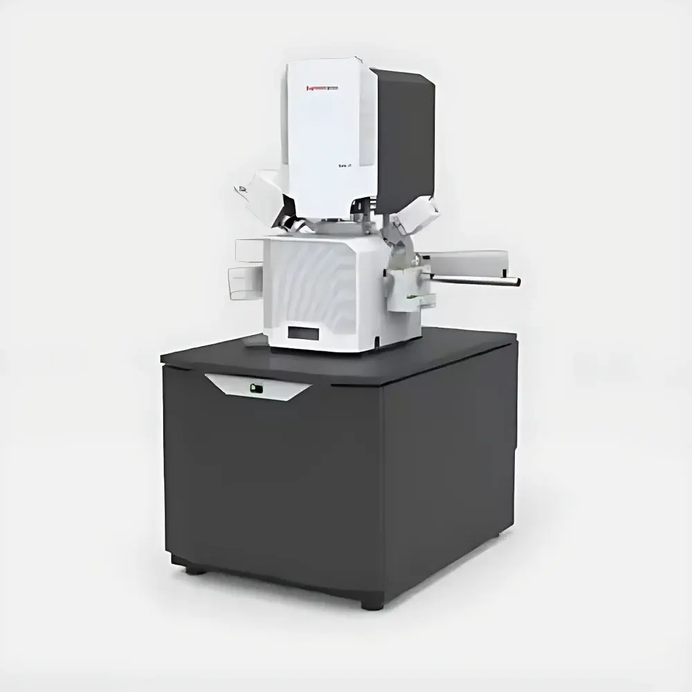
Thermo Scientific Apreo 2 SEM Field Emission Scanning Electron Microscope
| Brand | Thermo Fisher |
|---|---|
| Origin | Shanghai, China |
| Manufacturer Type | Authorized Distributor |
| Origin Category | Domestically Assembled (China) |
| Model | Thermo Scientific Apreo 2 SEM |
| Price | Upon Request |
| Resolution (30 kV) | 0.7 nm (STEM) |
| Resolution (15 kV) | 0.5 nm (with sample-stage deceleration) |
| Resolution (1 kV, 10 mm WD) | 1.0 nm (with deceleration) |
| Resolution (500 V) | 0.8 nm (with deceleration) |
| Landing Energy Range | 20 eV – 30 keV |
| Sample Stage | 5-axis motorized, ±90° tilt, 110 × 110 mm² XY travel |
| Max Sample Weight | 5 kg |
| Standard Detectors | ETD, T1, T2, T3, IR-CCD, Nav-Cam+ |
| Optional Detectors | DBS, LVD, DBS-GAD, STEM 3+, RGB-CLD, EDS, EBSD, WDS, Raman, EBIC |
| ColorSEM Technology | Real-time EDS-based elemental mapping integrated into imaging interface |
| SmartAlign & FLASH | Automated beam alignment, stigmation, and focus |
| Low Vacuum Mode | Optional, 10–500 Pa chamber pressure |
| Chamber Dimensions | 340 mm internal width, 12 ports, supports up to three EDS detectors (two at 180°), co-planar EDS/EBSD mounting orthogonal to tilt axis |
Overview
The Thermo Scientific Apreo 2 SEM is a high-performance field emission scanning electron microscope engineered for demanding materials characterization laboratories where resolution, usability, and analytical versatility must coexist without compromise. Operating on the principles of secondary electron (SE) and backscattered electron (BSE) detection—enhanced by in-lens and through-the-lens signal collection—the Apreo 2 delivers sub-nanometer spatial resolution across a broad landing energy range (20 eV to 30 keV). Its unique sample-stage deceleration technology enables high-resolution imaging at low accelerating voltages while maintaining optimal signal-to-noise ratio and surface sensitivity—critical for beam-sensitive polymers, biological coatings, and nanoscale thin films. Unlike conventional SEMs constrained by trade-offs between working distance and resolution, the Apreo 2 achieves 1.0 nm resolution at a 10 mm working distance under 1 kV decelerated conditions—a capability unmatched in its class. This eliminates the need for ultra-short working distances that limit detector geometry, stage maneuverability, and multi-technique integration.
Key Features
- Sub-nanometer resolution at extended working distances: Validated resolution of 0.5 nm at 15 kV (with deceleration) and 1.0 nm at 1 kV / 10 mm WD—enabling high-fidelity imaging with full detector accessibility and large-angle tilt compatibility.
- ColorSEM real-time elemental imaging: Fully integrated EDS engine delivers quantitative elemental maps overlaid directly onto SEM images—no post-acquisition processing or separate software workflows required. Supports point, line, and area analysis with Noran-style quantification protocols compliant with ISO 14722 and ASTM E1508 standards.
- SmartAlign and FLASH automation: Software-driven optical alignment, astigmatism correction, and focus optimization reduce operator dependency. New users achieve publication-grade imaging within minutes; experienced users preserve throughput during rapid technique switching.
- Modular detector architecture: Standard configuration includes Everhart-Thornley (ETD), three in-lens T-detectors (T1–T3), IR-CCD for cathodoluminescence preview, and Nav-Cam+ for contextual navigation. Optional detectors—including DBS, STEM 3+, EBSD, WDS, and Raman—mount co-planar to EDS and orthogonal to the tilt axis per ISO 21363 recommendations for angular reproducibility.
- Robust vacuum and stage design: 340 mm wide chamber with 12 dedicated ports supports simultaneous multi-detector configurations. The 5-axis motorized stage provides ±90° tilt, −15° to +90° rotation, 110 × 110 mm² XY travel, and 5 kg load capacity—compatible with cross-sectioned specimens, bulk metallurgical mounts, and in situ heating/cooling stages.
Sample Compatibility & Compliance
The Apreo 2 accommodates diverse specimen types—from conductive alloys and ceramic composites to non-conductive polymers, geological sections, and coated biological tissues—without mandatory sputter coating in many cases, thanks to low-voltage imaging and charge compensation via beam deceleration. Optional low-vacuum mode (10–500 Pa) extends applicability to hydrated, outgassing, or insulating samples. All hardware and software modules comply with IEC 61000-6-3 (EMC) and IEC 61010-1 (safety). Data acquisition and reporting workflows support audit-ready documentation per FDA 21 CFR Part 11 when configured with Thermo Scientific Connect software and electronic signature modules. Instrument calibration traceability aligns with NIST-traceable reference standards for resolution (e.g., SRM 2053a), beam current (SRM 2052), and energy dispersion (SRM 2054).
Software & Data Management
Control and analysis are unified under Thermo Scientific Maps software—built on a modular, API-accessible framework compatible with LabArchives ELN and Thermo Fisher’s broader Connect ecosystem. Maps supports GLP/GMP-compliant data handling: automatic metadata embedding (instrument ID, user, timestamp, acquisition parameters), version-controlled project archives, and encrypted export in TIFF, HDF5, and MRC formats. ColorSEM outputs include standardized .emsa and .eds files for third-party quantification (e.g., DTSA-II, Bruker Esprit). Batch processing, scripting (Python API), and remote operation via secure TLS-encrypted web interface enable centralized lab management and cross-site collaboration.
Applications
- Failure analysis of semiconductor interconnects and packaging defects
- Particle size and morphology characterization in battery cathode materials (e.g., NMC, LFP)
- In situ observation of grain boundary migration during thermal cycling
- Corrosion product phase identification using combined EDS/EBSD indexing
- 3D serial sectioning via FIB-SEM correlation workflows
- Quality control of additive-manufactured metal parts (porosity, unmelted powder, microcracks)
- Forensic analysis of gunshot residue and paint chip layering
FAQ
Does the Apreo 2 support EDS and EBSD simultaneously without geometric conflict?
Yes. The chamber port layout and detector mounting plane are designed per ISO 21363 Annex B to ensure co-planar EDS/EBSD installation orthogonal to the tilt axis—eliminating shadowing and enabling concurrent acquisition.
Is ColorSEM data compliant with ISO 14722 for quantitative elemental analysis?
ColorSEM uses Noran-style standardless quantification algorithms validated against certified reference materials (CRMs) and conforms to ISO 14722:2022 requirements for repeatability, detection limits, and matrix correction methodology.
Can the Apreo 2 operate in true low-vacuum mode below 1 kV?
Yes—low-vacuum mode (10–500 Pa) is fully functional down to 20 eV landing energy, enabling direct imaging of uncoated insulators and hydrated specimens with minimal charging artifacts.
What level of automation is available for routine QC workflows?
Maps software supports scriptable, parameter-locked acquisition sequences with pass/fail thresholds, auto-report generation (PDF/Excel), and integration with MES/QMS platforms via OPC UA or RESTful APIs.
How is beam stability maintained during long-duration EBSD mapping?
The Apreo 2 features active beam current stabilization (±0.5% over 8 hours) and drift-compensated stage control—validated per ASTM E3029 for positional accuracy in automated crystallographic mapping.


