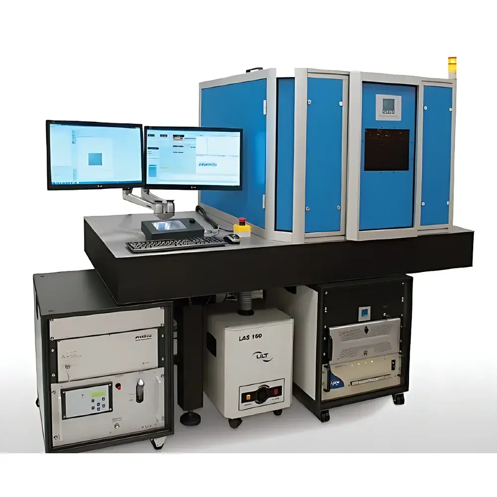
WOP FemtoLAB Femtosecond Laser Micro-Nanofabrication System
| Brand | WOP/Workshop of Photonics |
|---|---|
| Origin | Lithuania |
| Manufacturer Type | Authorized Distributor |
| Origin Category | Imported |
| Model | FemtoLAB |
| Price Range | USD 560,000 – 700,000 |
Overview
The WOP FemtoLAB Femtosecond Laser Micro-Nanofabrication System is a research-grade platform engineered for high-precision, non-thermal material processing at sub-micrometer spatial resolution. It operates on the principle of multiphoton absorption-driven ablation and polymerization, enabled by ultrashort laser pulses (typically < 500 fs pulse duration) centered at near-infrared wavelengths (e.g., 1030 nm or 515 nm via harmonic generation). Unlike nanosecond or picosecond lasers, femtosecond pulses deliver peak intensities exceeding 10¹²–10¹³ W/cm², inducing nonlinear optical interactions—such as dielectric breakdown, plasma formation, or two-photon initiated polymerization—without significant heat diffusion into adjacent regions. This results in minimal thermal damage, negligible recast layer formation, and sub-diffraction-limit feature definition—making the system suitable for maskless, direct-write fabrication of photonic crystals, microfluidic channels, MEMS components, plasmonic nanostructures, and bio-compatible scaffolds.
Key Features
- Integrated industrial-grade femtosecond fiber laser with adjustable repetition rate (1 kHz–5 MHz), pulse energy tuning (up to 50 µJ), and real-time pulse picker synchronization
- High-speed galvanometric scanning system with closed-loop position feedback, enabling scan speeds up to 10 m/s and positioning repeatability better than ±50 nm
- Motorized XYZ translation stage (±25 mm travel range, 10 nm step resolution) coupled with optional Z-axis piezo nanopositioner (100 µm range, 0.5 nm resolution)
- Beam delivery optics featuring diffraction-limited focusing (NA ≥ 0.8), achromatic collimation, and active beam stabilization
- Dedicated hardware-triggered shutter and pulse-on-demand control for single-pulse-per-position ablation
- Modular architecture supporting optional add-ons: time-resolved fluorescence detection module, in-situ Raman monitoring head, or vacuum-compatible chamber interface
Sample Compatibility & Compliance
The FemtoLAB accommodates a broad spectrum of substrates—including fused silica, sapphire, silicon wafers (up to 200 mm diameter), ITO-coated glass, SU-8 and IP-L photoresists, hydrogels, and biological tissues—without requiring conductive coatings or vacuum environments. Its open-access optical path allows integration with external metrology tools (e.g., white-light interferometry, SEM alignment ports). The system conforms to CE marking requirements under Directive 2006/42/EC (Machinery Directive) and 2014/30/EU (EMC Directive). All laser safety interlocks comply with IEC 60825-1:2014 Class 4 laser product standards. For regulated environments, optional audit trail logging, user access levels, and electronic signature support align with FDA 21 CFR Part 11 and ISO/IEC 17025 traceability frameworks.
Software & Data Management
Control and workflow orchestration are managed through WOP’s proprietary FemtoControl Suite—a Windows-based application built on Qt and Python APIs. It supports G-code import, parametric pattern generation (including fractal, spiral, and lattice-based designs), real-time power calibration curves, and multi-layer stacking with layer-specific fluence mapping. Raw acquisition data (pulse count, stage coordinates, laser energy per shot, environmental sensor logs) are stored in HDF5 format with embedded metadata compliant with FAIR principles. Export options include STL (for 3D structures), SVG (for 2D vector patterns), and CSV (for statistical process control). Remote monitoring via TLS-secured WebSocket API enables integration into lab-wide LIMS or MES platforms.
Applications
- Direct-write fabrication of photonic bandgap structures and integrated waveguides in bulk glasses and crystals
- Microstructuring of electrode surfaces for next-generation batteries and fuel cells
- Creation of high-aspect-ratio microchannels and valves in PDMS and thermoplastics for organ-on-chip devices
- Nanoscale surface texturing of biomedical implants to modulate cell adhesion and protein adsorption
- Maskless prototyping of diffractive optical elements (DOEs) and metasurfaces with feature sizes down to 180 nm
- In-situ modification of 2D materials (e.g., graphene, MoS₂) for localized doping or defect engineering
FAQ
What is the typical minimum feature size achievable with the FemtoLAB system?
Sub-200 nm features can be routinely fabricated in optimized photoresists (e.g., IP-L 780) using tightly focused beams and precise dose control; actual resolution depends on material nonlinearity, numerical aperture, and pulse energy stability.
Can the system perform both ablation and two-photon polymerization in the same setup?
Yes—the platform supports interchangeable optical configurations: high-peak-power mode for ablation and low-energy, high-repetition-rate mode for multiphoton lithography, both controlled via software-defined parameter sets.
Is remote operation supported for multi-user academic or shared-facility environments?
The system includes VNC-enabled remote desktop access and RESTful API endpoints for job queuing, status polling, and error reporting—fully compatible with university HPC cluster schedulers and centralized instrument management portals.
Does WOP provide application-specific process development support?
WOP offers collaborative feasibility studies, including material response characterization, threshold fluence mapping, and post-processing protocol optimization—delivered as documented SOPs aligned with ISO 13485 or ASTM F2792 standards where applicable.


