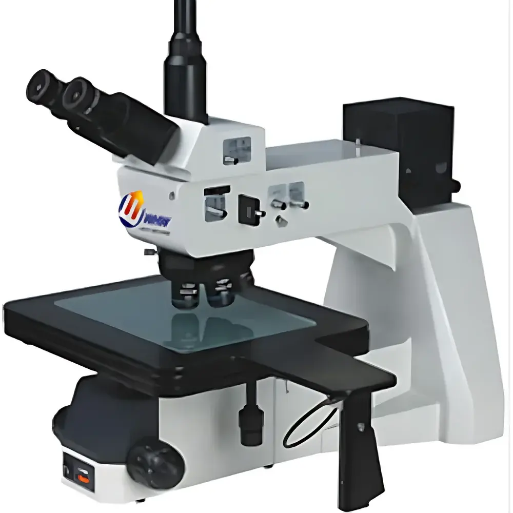
YANRUN 8XB Large-Platform Chip Inspection Metallurgical Microscope
| Brand | YANRUN |
|---|---|
| Origin | Shanghai, China |
| Manufacturer Type | Direct Manufacturer |
| Product Type | Upright Metallurgical Microscope |
| Eyepieces | WF10× (25 mm FOV), WF10× (20 mm FOV) with 0.1 mm十字 crosshair reticle |
| Nosepiece | Five-position brightfield/darkfield turret with DIC slots |
| Objectives | Plan infinity-corrected BF/DF objectives — 5×/0.1 BD, WD 29.4 mm |
| Stage | Dual-layer mechanical stage (350 × 310 mm base, 250 × 250 mm travel range) |
| Focus Mechanism | Coaxial coarse/fine focus with rack-and-pinion drive |
| fine focus graduation | 2 µm |
| Illumination | Episcopic halogen lamp (12 V / 100 W), AC 85–230 V, adjustable intensity, equipped with aperture and field diaphragms |
| Polarization System | Rotatable analyzer (0–360°), removable polarizer and analyzer |
| Filters | Slide-in blue, green, neutral density filters |
| Calibration Tool | 0.01 mm stage micrometer |
| Standard Accessories | Microscope body, observation tube, pair of WF10× eyepieces, four BF/DF objectives (5×, 10×, 20×, 40×), one 12 V / 100 W halogen bulb, full polarization kit, filter set, calibration micrometer, certificate of conformity, warranty card, and user manual |
Overview
The YANRUN 8XB Large-Platform Chip Inspection Metallurgical Microscope is an upright, high-stability optical instrument engineered for precise microstructural analysis of semiconductor wafers, integrated circuit packages, solder joints, metallized layers, and other planar microelectronic components. Designed around an infinite-conjugate optical pathway with plan-apochromatic correction, the system delivers high-resolution, high-contrast imaging under both brightfield (BF) and darkfield (DF) illumination modes—critical for detecting subsurface defects, grain boundaries, intermetallic phases, and surface topography in conductive and reflective specimens. Its episcopic illumination architecture eliminates the need for specimen thinning or sectioning, enabling non-destructive evaluation directly on packaged chips, PCB substrates, and bond pads. The microscope conforms to ISO 10934-1 (optical microscopy terminology) and supports traceable metrology through calibrated stage movement and reticle-based measurement protocols.
Key Features
- Large-format mechanical stage (350 mm × 310 mm base, 250 mm × 250 mm travel range) accommodates full 300 mm wafers and multi-die test boards without repositioning.
- Five-position objective turret with dedicated slots for Differential Interference Contrast (DIC) modules—enabling optional phase-gradient contrast enhancement without optical path realignment.
- Plan infinity-corrected brightfield/darkfield objectives (5×, 10×, 20×, 40×) optimized for high numerical aperture and long working distance—ensuring compatibility with probe stations and automated handling fixtures.
- Coaxial coarse/fine focusing mechanism with 2 µm fine-focus graduation and backlash-free rack-and-pinion transmission for repeatable Z-axis positioning during focus stacking or depth profiling.
- Dual-mode polarization system featuring a 360° rotatable analyzer and fully retractable polarizer/analyzer elements—supporting birefringence mapping of stress-induced crystal lattice distortion in silicon and compound semiconductors.
- Adjustable episcopic halogen illumination (12 V / 100 W) with independent aperture and field diaphragms for Köhler illumination optimization and glare suppression on highly reflective surfaces.
Sample Compatibility & Compliance
The 8XB accepts standard semiconductor-grade specimens—including bare dies, flip-chip assemblies, wire-bonded packages, ceramic substrates, and metal-coated photomasks—without requiring immersion media or conductive coating. Its long-working-distance optics and wide-stage clearance support integration with external probing systems and environmental chambers. The system complies with IEC 61000-4-2 (ESD immunity) and meets CE marking requirements for laboratory optical equipment. While not supplied with image analysis software, the optical train is compatible with third-party machine vision cameras (C-mount interface) and adheres to ANSI Z80.10-2020 standards for microscope mechanical stability and optical alignment repeatability.
Software & Data Management
The YANRUN 8XB operates as a hardware platform for standalone visual inspection or as a peripheral device in automated QA workflows. It features standardized C-mount threading (1.0× magnification factor) for seamless integration with USB3.0 or GigE industrial cameras. When paired with validated image acquisition software (e.g., Stream Motion, Olympus cellSens, or open-source Micro-Manager), the system supports time-lapse capture, multi-point coordinate logging, and GLP-compliant metadata embedding—including operator ID, timestamp, objective ID, and stage coordinates. Audit trails and electronic signatures may be implemented via external LIMS or ELN platforms compliant with FDA 21 CFR Part 11 when used in regulated semiconductor manufacturing environments.
Applications
- Failure analysis of solder voids, die attach delamination, and wire bond lift-off in IC packaging.
- Grain size quantification and phase distribution mapping in copper-tungsten metallization layers per ASTM E112.
- Surface roughness assessment and defect classification (scratches, pits, residues) on polished SiC and GaN wafers.
- Qualitative birefringence evaluation of thermally induced stress in passivation films (e.g., SiO₂, Si₃N₄).
- Dimensional verification of lithographic features using calibrated reticle measurements and stage micrometers.
- Pre- and post-reliability testing inspection (e.g., temperature cycling, HAST, TCT) per JEDEC JESD22-A108.
FAQ
Does the 8XB include digital imaging capability out of the box?
No—the system ships without a camera or image analysis software. It is configured for direct visual observation and manual measurement using the included crosshair eyepieces and stage micrometer.
Can the microscope be upgraded to support DIC or fluorescence?
DIC functionality is supported via optional DIC sliders compatible with the turret’s dedicated slots. Fluorescence is not natively supported due to the absence of excitation filter cubes and mercury/xenon lamp housing.
What is the maximum specimen height clearance above the stage?
With all standard objectives mounted, vertical clearance from stage surface to objective front lens exceeds 55 mm at 5× magnification—sufficient for most probe cards and thermal chucks.
Is calibration documentation provided for metrological use?
Yes—a NIST-traceable 0.01 mm stage micrometer is included, and the reticle scale is factory-verified against ISO 7888 reference standards.
Are service and technical support available outside mainland China?
YANRUN provides remote diagnostic support and authorized distributor networks in Southeast Asia, the Middle East, and select EU markets; extended warranty and on-site service contracts are negotiable under OEM agreements.


