ZEPTOOLS JS3000B Automated Stylus Profilometer
| Brand | ZEPTOOLS |
|---|---|
| Origin | Anhui, China |
| Model | JS3000B |
| Positioning Accuracy | < ±10 µm |
| Probe Tip Radius | ≥2 µm (60° included angle, standard) |
| Probe Normal Force Range | 0.5–50 mg |
| Scan Length | ≤55 mm |
| Step Height Repeatability | ≤0.5 nm |
| Vertical Resolution | 0.05 nm |
| Maximum Step Height Range | ≤80 µm |
| Wafer Compatibility | 200 mm & 300 mm (thickness ≤10 mm |
| materials | Si, LiTaO₃, glass, opaque/semi-transparent/transparent substrates) |
| Image Recognition Localization Accuracy | < ±10 µm |
| Mechanical Stability | >500 wafers in continuous EFEM transfer test |
| Throughput | ≥10 WPH (single-side, ≥5 measurement sites) |
Overview
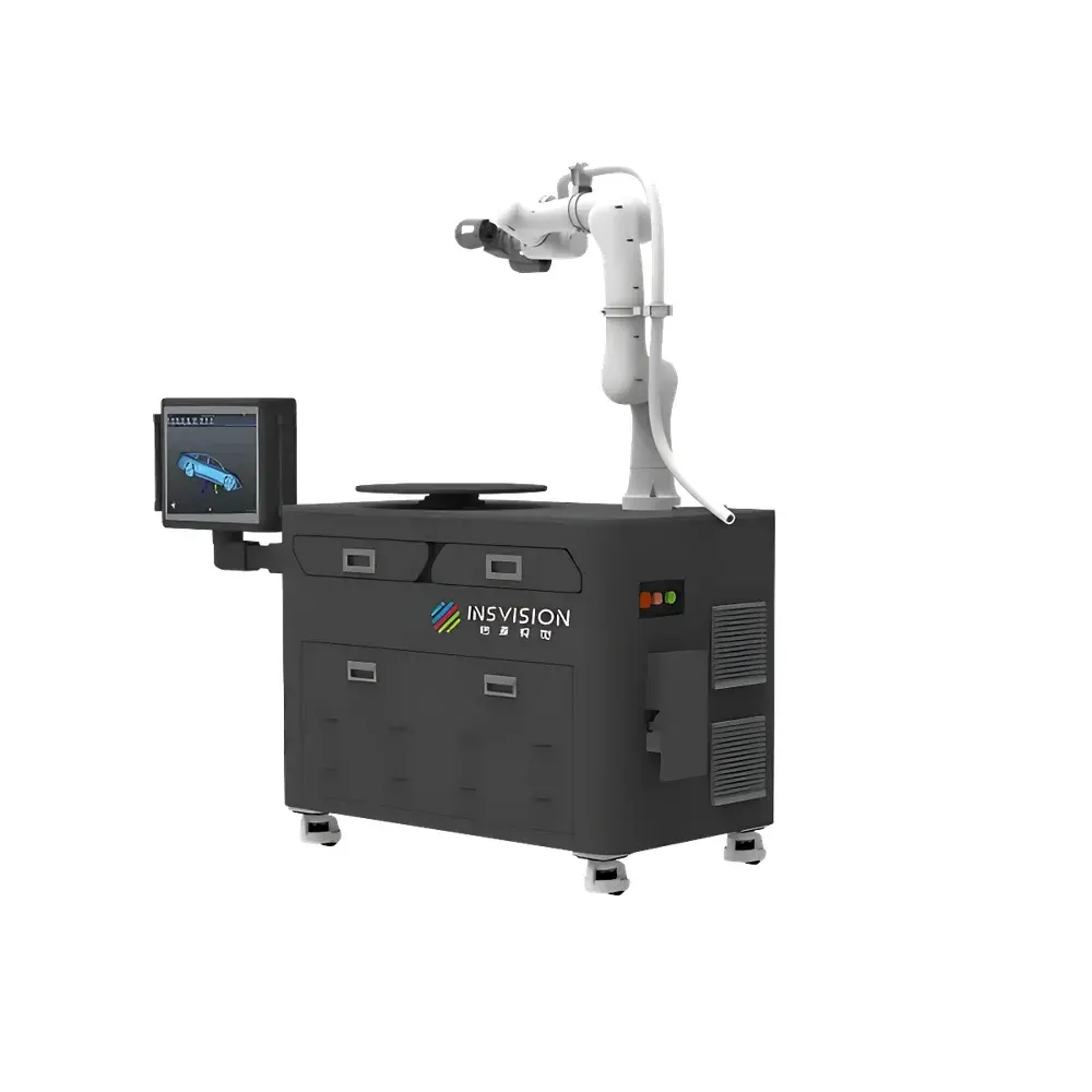
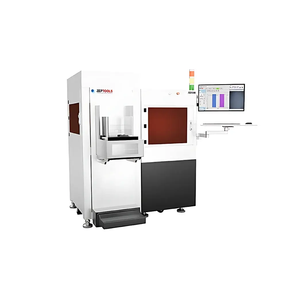
The ZEPTOOLS JS3000B Automated Stylus Profilometer is a high-precision contact-based surface metrology instrument engineered for nanoscale topographic characterization of micro- and nanostructured surfaces. It operates on the principle of mechanical scanning profilometry: a diamond-tipped stylus physically traverses the sample surface under precisely regulated normal force, converting vertical displacement into high-fidelity analog signals via a high-stability differential inductive sensor. These signals are digitized and processed using real-time feedback-controlled servo electronics to resolve sub-nanometer vertical features with exceptional linearity and thermal stability. Designed for integration into cleanroom environments, the JS3000B supports automated wafer handling via EFEM (Equipment Front End Module) architecture—comprising Load Port (LP), robotic arm, and auto-alignment unit—enabling unattended operation in semiconductor fabrication labs, R&D centers, and quality control facilities. Its core measurement capabilities include step height, film thickness (via etch-depth or deposition-height profiling), surface roughness (Ra, Rq, Rz per ISO 4287/ISO 25178), waviness, flatness, warpage, and thin-film stress analysis (using Stoney’s equation with multi-point curvature mapping).
Key Features
- Ultra-low-force probing system with closed-loop force regulation (0.5–50 mg range), minimizing plastic deformation on soft polymers, photoresists, and low-modulus dielectrics while maintaining signal integrity on hard substrates.
- Sub-nanometer vertical resolution (0.05 nm) and ≤0.5 nm step height repeatability—validated per ISO 25178-602 and ASTM E2923 guidelines for profilometer calibration and verification.
- Integrated coaxial optical imaging subsystem with motorized zoom and real-time probe–sample positional overlay, enabling precise feature targeting without manual repositioning.
- Modular EFEM-ready design compliant with SEMI E84 (SECS/GEM) standards, supporting seamless integration into 300 mm fab automation workflows including recipe-driven multi-site scanning and batch data export.
- Thermally stable granite base and air-isolated optical stage reduce environmental drift; mechanical endurance verified over >500 consecutive wafer transfers in marathon testing.
- Standard 60° conical diamond probe (tip radius ≥2 µm); optional sub-micron probe (radius ≤1 µm) available for high-aspect-ratio trench and sidewall profiling.
Sample Compatibility & Compliance
The JS3000B accommodates wafers up to 300 mm (12 inch) in diameter and ≤10 mm thickness, including silicon, lithium tantalate (LiTaO₃), fused silica, quartz, and patterned glass substrates—regardless of optical transparency. Its non-vacuum, ambient-air operating environment eliminates outgassing concerns associated with electron-beam tools, making it suitable for organic layers, metal oxides, and bio-coated surfaces. All measurement protocols adhere to ISO/IEC 17025 traceability requirements when used with NIST-traceable step height reference standards (e.g., NIST SRM 2160). Software audit trails comply with FDA 21 CFR Part 11 for electronic records and signatures where configured with user authentication, role-based access, and immutable data logging.
Software & Data Management
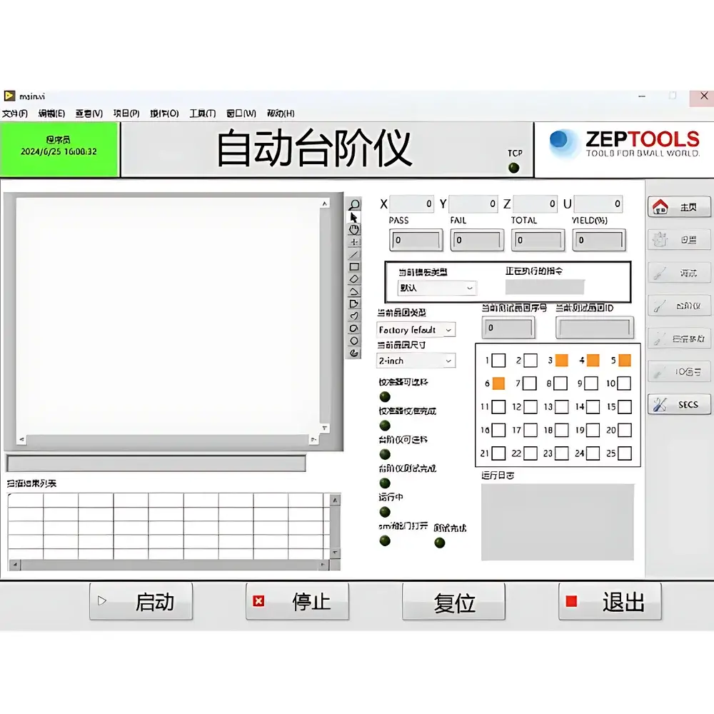
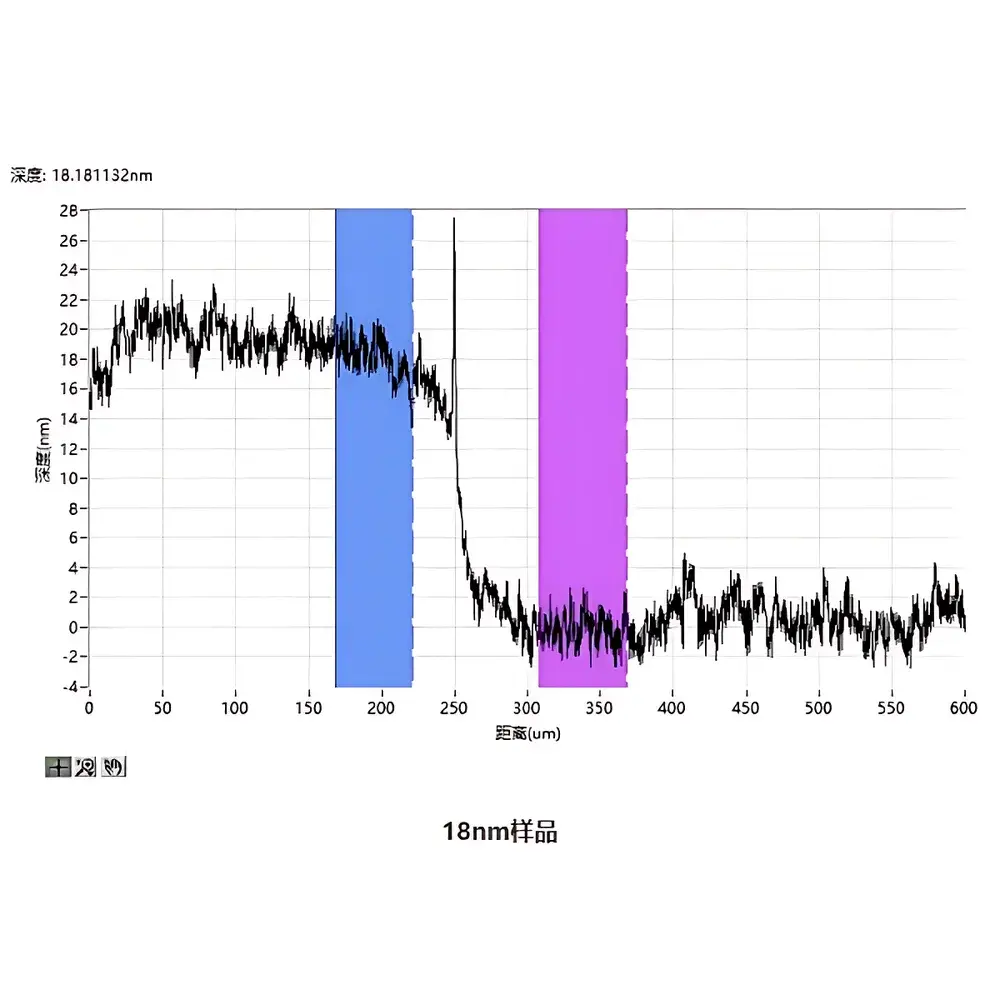
ZEPTOOLS ProfilSoft™ v5.2 provides full control of acquisition, analysis, and reporting. It supports ISO-compliant roughness parameters (Ra, Rq, Rsk, Rku, Rz), step height quantification with edge-detection algorithms (tangent, threshold, centroid), 3D surface reconstruction, curvature-derived stress calculation, and warpage vector mapping. Data export formats include CSV, ASCII, STP, and Metrology Markup Language (MMML) for interoperability with MES and SPC platforms. Batch processing enables scheduled execution across hundreds of predefined sites on multiple wafers, with automated pass/fail flagging against user-defined tolerance bands. Raw data files retain full metadata—including timestamp, probe ID, force setting, scan velocity, and environmental logs—for GLP/GMP audit readiness.
Applications
- Thin-film process control: measuring etch depth uniformity, CVD/PVD film thickness, and post-CMP dishing/erosion.
- MEMS and advanced packaging: characterizing release etch profiles, bond interface topography, and TSV sidewall roughness.
- LED and power device manufacturing: quantifying epitaxial layer steps, mesa isolation heights, and solder bump coplanarity.
- Photomask and reticle inspection support: verifying chrome etch depth and resist development profiles.
- Academic and national lab research: nanomechanical property correlation via controlled-force indentation profiling and viscoelastic surface response analysis.
FAQ
What standards does the JS3000B comply with for calibration and measurement uncertainty?
The system conforms to ISO 25178-602 (areal surface texture calibration), ISO 4287 (profile roughness), and ASTM E2923 (profilometer performance verification). Traceable calibration is achievable using certified step height standards (e.g., NIST SRM 2160, VLSI Standards VS-100 series).
Can the JS3000B measure transparent or semi-transparent films on glass substrates?
Yes—unlike optical interferometers, contact profilometry is insensitive to substrate optical properties. The JS3000B directly measures physical topography regardless of refractive index or transmission characteristics.
Is the software validated for regulated environments (e.g., ISO 13485, IEC 62304)?
ProfilSoft™ supports 21 CFR Part 11 compliance when deployed with network-authenticated login, electronic signature workflows, and tamper-evident audit logs—fully configurable for medical device or pharmaceutical QC laboratories.
What maintenance intervals are recommended for long-term metrological stability?
Annual calibration verification is recommended; probe tip wear inspection every 200 hours of active scanning; granite base leveling and environmental vibration assessment quarterly in high-precision installations.
Does the system support custom scripting for automated metrology recipes?
Yes—ProfilSoft™ exposes COM/ActiveX interfaces and Python-compatible API libraries, enabling integration with LabVIEW, MATLAB, or proprietary factory automation systems for adaptive measurement logic.