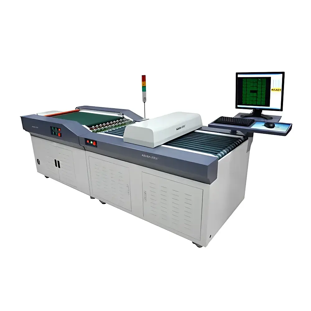
Zhengye JK5200 PCB Hole Inspection System
| Brand | Zhengye |
|---|---|
| Origin | Guangdong, China |
| Manufacturer Type | Direct Manufacturer |
| Country of Origin | China |
| Model | JK5200 |
| Pricing | Upon Request |
| Detection Speed | 3.0–12.5 m/min (configurable by mode) |
| Repeatability | ±30 µm (standard holes), ±75 µm (slot length/width), ±150 µm (irregular holes) |
| Measurement Accuracy | ±20 µm (hole diameter ≤1 mm), ±30 µm (1 mm < Ø < 4 mm), ±40 µm (Ø > 4 mm) |
| Hole Diameter Range | 0.1–10 mm |
| Board Format | 80 × 100 mm to 630 × 650 mm |
| Board Thickness | 0.3–10 mm |
| Minimum Edge-to-Hole Distance | ≥0.10 mm |
| Dimensions (L×W×H) | 3510 × 1160 × 1100 mm |
| Weight | ~800 kg |
Overview
The Zhengye JK5200 PCB Hole Inspection System is an automated optical inspection platform engineered for high-precision metrology and defect classification in printed circuit board (PCB) manufacturing. It operates on the principle of high-resolution contact image sensor (CIS)-based scanning combined with real-time sub-pixel edge detection and geometric feature extraction algorithms. Designed for integration into post-drilling and pre-packaging process lines, the system performs non-contact, full-surface measurement of drilled hole count, positional accuracy, dimensional conformity, and surface-level anomalies—including plugged vias, foreign material intrusion, slot elongation or truncation, and misshapen apertures. Its dual-lane architecture supports concurrent inspection of two PCBs, enabling throughput scalability without compromising measurement integrity. The system complies with IPC-A-600 and IPC-6012 requirements for via and plated-through-hole (PTH) acceptability criteria, and its measurement traceability aligns with ISO/IEC 17025 principles for in-house calibration verification.
Key Features
- High-fidelity CIS imaging module with 5 µm effective pixel resolution and uniform illumination across the full scan field, minimizing parallax-induced distortion and ensuring consistent contrast for copper, solder mask, and substrate surfaces.
- Dual independent inspection lanes with synchronized conveyor control, allowing parallel processing of boards up to 630 × 650 mm—increasing line efficiency while maintaining per-board data isolation.
- Adaptive thresholding and multi-scale morphological analysis for robust detection of subtle defects such as micro-plugging (<50 µm residual height), partial debris occlusion, and slot asymmetry below 10 µm deviation.
- Networked diagnostic station functionality: NG boards are automatically flagged with georeferenced defect maps; remote terminals access real-time thumbnails, coordinate metadata, and classification confidence scores via standard HTTP/HTTPS interfaces—enabling cross-shift engineering review without physical board retrieval.
- Modular software architecture supporting user-defined pass/fail rulesets based on IPC Class II/III tolerances, including dynamic tolerance bands that scale with nominal hole size and board thickness.
Sample Compatibility & Compliance
The JK5200 accommodates rigid, flex-rigid, and metal-core PCBs within a thickness range of 0.3–10 mm and aspect ratios up to 12:1. It supports both single-sided and double-sided drilling verification, with automatic top/bottom surface registration using fiducial-based alignment. All measurements adhere to IPC-TM-650 Test Methods 2.2.12 (optical measurement of hole dimensions) and 2.2.15 (defect classification). System validation documentation includes Gage R&R studies per AIAG MSA guidelines, with reported repeatability values meeting ≤10% of total tolerance for critical PTH features. The mechanical frame conforms to CE machinery directive (2006/42/EC) and EMC directive (2014/30/EU); safety interlocks meet ISO 13857 requirements.
Software & Data Management
The embedded inspection software runs on a real-time Linux OS with deterministic I/O scheduling, ensuring jitter-free image acquisition at maximum belt speeds. Data output includes CSV-formatted metrology logs, PNG-based annotated defect overlays, and XML reports compliant with IPC-2581B schema for seamless integration into MES platforms (e.g., Siemens Opcenter, Rockwell FactoryTalk). Audit trails record operator logins, parameter modifications, and result overrides with timestamped digital signatures. Optional FDA 21 CFR Part 11 compliance package provides electronic signature enforcement, role-based access control, and immutable archival of raw images and processed results for GLP/GMP-regulated facilities.
Applications
- Final QA gate for HDI and multilayer PCBs prior to electroplating or solder mask application.
- In-process verification after CNC drilling or laser ablation—identifying tool wear patterns through statistical trend analysis of hole roundness and centroid drift.
- Root cause analysis support for lamination voids or drill bit deflection by correlating localized hole deformation clusters with CAD netlist coordinates.
- Supplier qualification audits requiring objective, quantifiable evidence of hole geometry conformance across batch lots.
- Process capability assessment (Cpk/Ppk) for critical hole populations using SPC charts generated directly from inspection database queries.
FAQ
Does the JK5200 support automatic calibration verification?
Yes—the system includes a NIST-traceable ceramic reference plate with certified hole arrays (Ø 0.2 mm to 6.0 mm) for daily performance checks. Calibration status is logged and exportable.
Can it inspect laser-drilled microvias (≤100 µm)?
It detects microvias down to 0.1 mm (100 µm) with quantitative measurement; however, sub-75 µm features fall below the validated repeatability threshold and are classified as presence/absence only.
Is offline programming supported for new board designs?
Yes—Gerber RS-274X and ODB++ import modules enable offline recipe generation, including custom ROI definition, tolerance mapping, and defect severity weighting.
What network protocols does the remote diagnostic station use?
HTTP/HTTPS for web-based viewing; optional OPC UA server for real-time data streaming to SCADA or historian systems.
How is measurement uncertainty documented for quality audits?
Each inspection report includes an embedded uncertainty budget per IPC-2581B Annex D, listing contributions from optics, motion control, algorithmic segmentation, and environmental temperature drift (±0.5°C compensated).
Related Products

 and Vehicle Classification System")