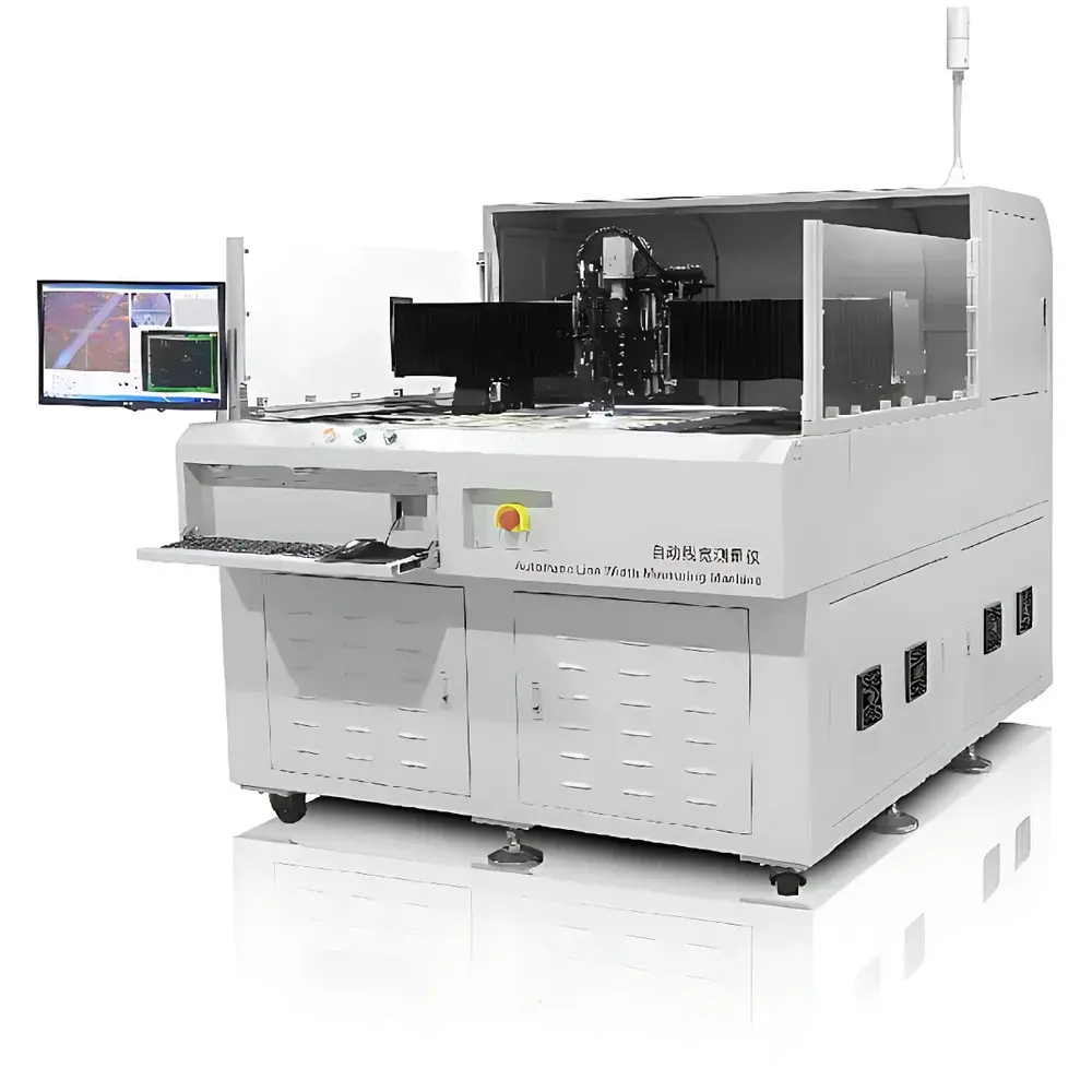
Zhengye PCBXK32A Automated Line Width Measurement System
| Brand | Zhengye |
|---|---|
| Origin | Guangdong, China |
| Manufacturer Type | OEM/ODM Manufacturer |
| Country of Origin | China |
| Model | PCBXK32A |
| Pricing | Available Upon Request |
Overview
The Zhengye PCBXK32A Automated Line Width Measurement System is a precision optical metrology instrument engineered for non-contact, high-resolution dimensional analysis of printed circuit board (PCB) features. It operates on the principle of high-magnification digital imaging combined with calibrated machine vision algorithms to quantify critical geometric parameters—including line width (top and bottom), line spacing (pitch), circular via diameters, and gold finger trace widths—on both inner and outer layer PCB substrates post-etching and pre-solder mask application. Designed specifically to meet the stringent dimensional tolerances demanded by 5G RF boards, HDI (High-Density Interconnect), and advanced packaging substrates, the system delivers repeatable sub-micron measurement capability within its field of view. Its vertical coaxial illumination architecture ensures uniform contrast across copper traces and etch profiles, minimizing shadowing artifacts and enabling robust edge detection even on low-contrast or oxidized surfaces.
Key Features
- Fourth-generation platform with upgraded optical train: includes 12 MP industrial CMOS sensor, telecentric lens assembly, and programmable multi-angle LED ring illumination for optimal edge definition
- Automated stage with ±0.5 µm positional repeatability and 300 × 300 mm travel range, supporting full-panel scanning of standard PCB sizes up to 18″ × 24″
- Real-time image acquisition at ≥30 fps with hardware-triggered synchronization to stage motion, enabling seamless stitching of large-area measurements
- Embedded calibration engine compliant with ISO 17025 traceability requirements; supports NIST-traceable reference standards for line width and pitch verification
- Rugged industrial enclosure rated IP54, designed for continuous operation in Class 10,000 cleanroom environments typical of PCB fabrication facilities
- Integrated thermal management system maintains optical path stability across ambient temperatures from 20–26 °C, ensuring long-term measurement consistency
Sample Compatibility & Compliance
The PCBXK32A accommodates rigid, flex, and rigid-flex PCBs with substrate thicknesses ranging from 0.05 mm to 3.2 mm and surface finishes including bare copper, ENIG, ENEPIG, immersion silver, and OSP. It supports measurement of features as narrow as 25 µm (line width) and as small as 50 µm (via diameter) within a single field of view (FOV: 2.5 mm × 2.5 mm at highest magnification). The system conforms to IPC-TM-650 Test Methods 2.2.15 (Optical Microscopy) and 2.2.17 (Image Analysis), and its measurement uncertainty budget is documented per ISO/IEC 17025:2017 Annex A.5 guidelines. All measurement data logs include timestamp, operator ID, calibration status, and environmental metadata required for GLP/GMP audit readiness.
Software & Data Management
The proprietary Zhengye VisionMaster™ v4.2 software provides a validated, CFR Part 11-compliant environment with role-based access control, electronic signatures, and full audit trail functionality. Measurement workflows are fully scriptable via Python API, enabling integration into MES (Manufacturing Execution Systems) and SPC (Statistical Process Control) platforms. Reports export in PDF/A-1b, CSV, and XML formats—with embedded measurement images, tolerance overlays, and CPK/PPK statistical summaries. Data retention policies support automated archiving to network-attached storage (NAS) or cloud-based repositories with AES-256 encryption. Software validation documentation (IQ/OQ/PQ protocols) is available upon request for regulated manufacturing environments.
Applications
- Inline quality verification of etched copper patterns during inner/outer layer fabrication
- Process capability assessment for fine-line lithography (≤50 µm L/S) in 5G mmWave antenna modules
- Root cause analysis of undercut/over-etch defects via top-bottom width ratio trending
- First-article inspection (FAI) and PPAP submission support for automotive and aerospace PCB suppliers
- Green solder mask alignment verification through fiducial overlay analysis
- Failure analysis lab use for cross-sectional correlation studies using registered optical-to-SEM coordinate mapping
FAQ
What is the minimum measurable line width supported by the PCBXK32A?
The system achieves reliable detection and measurement of copper traces down to 25 µm nominal width under standard lighting and focus conditions.
Does the system support automatic defect classification (e.g., bridging, open circuit)?
Yes—VisionMaster™ includes configurable rule-based defect classification engines that classify anomalies per IPC-A-600 criteria, with customizable pass/fail thresholds.
Is the software compliant with FDA 21 CFR Part 11 requirements?
Yes—the software includes full electronic signature implementation, audit trail logging, and secure user authentication aligned with Part 11 Annex A guidance.
Can the system be integrated into an existing factory automation infrastructure?
Yes—it supports Modbus TCP, OPC UA, and RESTful API interfaces for bi-directional communication with PLCs, MES, and SCADA systems.
What calibration standards are recommended for routine verification?
Zhengye recommends quarterly verification using certified photomask standards traceable to NIST SRM 2059 (Line Width Standards) or equivalent national metrology institute references.