Zhengye X-Ray Inspection System for Non-Destructive Internal Structure Analysis of Semiconductor Devices
| Brand | Zhengye |
|---|---|
| Origin | Guangdong, China |
| Manufacturer Type | Original Equipment Manufacturer (OEM) |
| Product Origin | Domestic (China) |
| Model | Zhengye X-Ray Inspection System |
| Pricing | Available Upon Request |
Overview
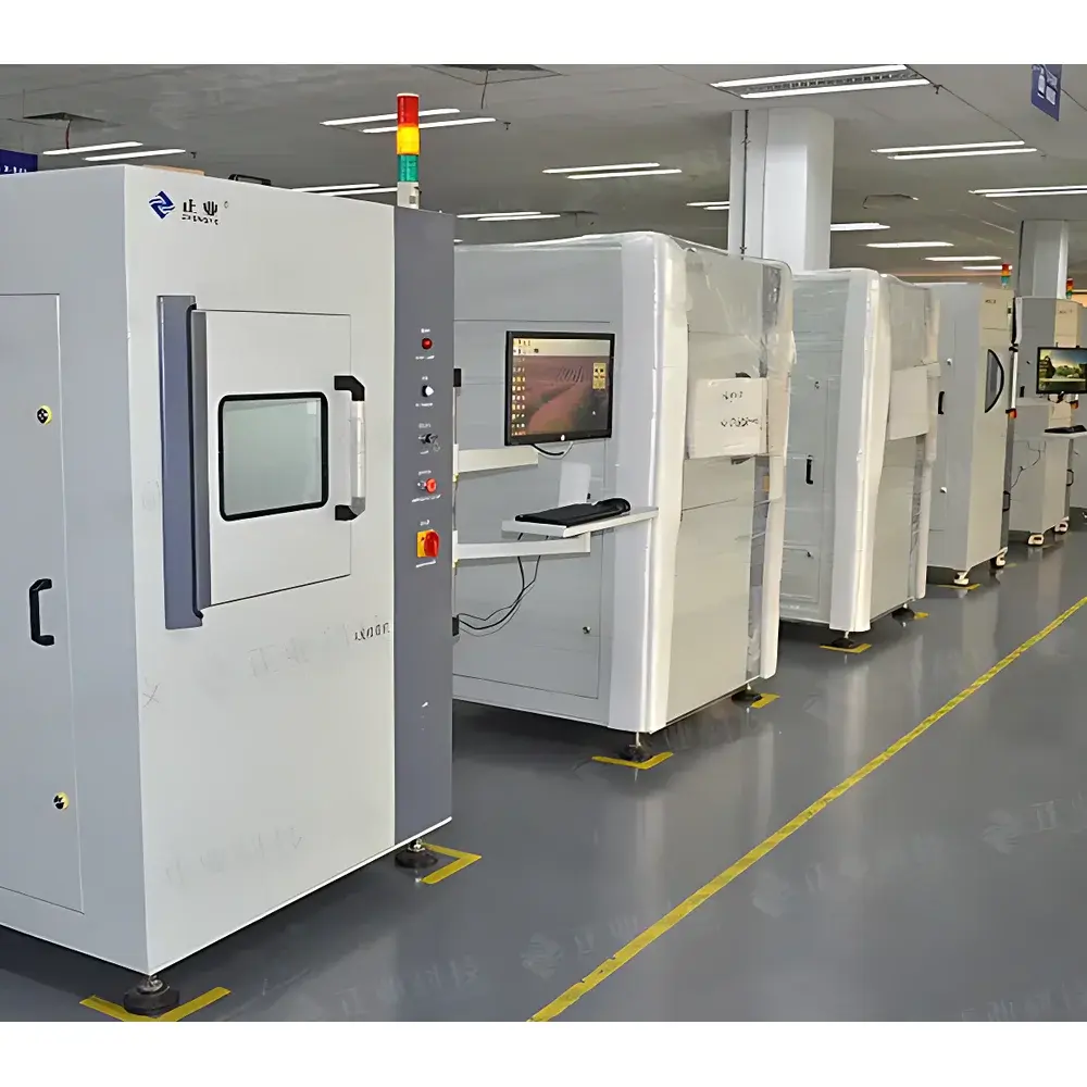
The Zhengye X-Ray Inspection System is a high-precision, non-destructive testing (NDT) platform engineered specifically for semiconductor device characterization and failure analysis. Utilizing digital radiographic imaging based on X-ray transmission physics, the system enables real-time, high-resolution visualization of internal structural features—including bond wire integrity, die attach voids, package delamination, solder joint morphology, and interconnect anomalies—without physical sectioning or sample destruction. Designed for integration into semiconductor front-end and back-end process control environments, it supports both R&D validation and inline quality assurance workflows. The system operates in accordance with fundamental X-ray attenuation principles governed by Beer-Lambert law, where differential absorption across material densities generates contrast in the projected image, enabling quantitative defect discrimination at sub-50 µm feature resolution under optimal configuration.
Key Features
- 2.5D Metrology Capability: Supports precise geometric measurements including linear distance, circle diameter, concentricity evaluation, and point-to-center distance—enabling dimensional verification of bond pads, lead frames, and encapsulation features.
- CNC Path Programming: Integrated motion control allows users to record, store, and replay inspection trajectories with micron-level repeatability; ideal for batch inspection of low-volume, high-mix semiconductor packages (e.g., QFN, BGA, WLCSP).
- Intelligent Navigation Interface: Features a large-field-of-view navigation window synchronized with high-magnification imaging; click-to-position functionality enables rapid targeting of regions of interest (ROIs) with automated stage repositioning.
- Triaxial Detector & Source Motion: Independent X-Y-Z movement of X-ray tube and image intensifier/detector assembly ensures optimal geometric magnification (Mg = 1 + SOD/SDD), minimizing parallax error and maximizing spatial fidelity.
- Mechanical Architecture: Precision motion system employs ground-grade ball screws, timing belt-driven stepper motors, and rigid aluminum alloy frame—designed for long-term stability, vibration damping, and thermal drift compensation.
Sample Compatibility & Compliance
The system accommodates standard semiconductor packaging formats up to 300 mm × 300 mm footprint, including wafers (with carrier support), singulated dies, leaded and leadless IC packages, power modules, and MEMS assemblies. It complies with IEC 61000-6-3 (EMC emissions), IEC 61000-6-2 (immunity), and meets Class I laser safety requirements per IEC 60825-1 when equipped with optional laser alignment aids. While not certified for medical use, its radiation shielding design conforms to national GBZ 138–2002 standards for industrial X-ray equipment, ensuring operator safety during routine operation. Data integrity protocols align with GLP/GMP documentation expectations, supporting audit-ready traceability for internal QA processes.
Software & Data Management
The proprietary inspection software provides full workflow automation—from acquisition and measurement to pass/fail decision logic and report generation. Image data is stored in DICOM-compliant format and supports TIFF, BMP, and PNG export. Real-time image enhancement includes dynamic range compression, edge sharpening, noise reduction, and contrast-limited adaptive histogram equalization (CLAHE). Measurement results are logged with timestamp, operator ID, and machine parameters; audit trail functionality records all user actions per ISO/IEC 17025:2017 Annex A.2 guidelines. Exported reports include annotated images, statistical summaries (mean, std dev, Cp/Cpk), and CSV-compatible metrology tables suitable for SPC integration.
Applications
- Fault isolation in flip-chip and wire-bond interconnects
- Void quantification in underfill and mold compound layers
- Die tilt and warpage assessment in advanced packaging (2.5D/3D IC)
- Lead frame coplanarity verification prior to surface-mount assembly
- Post-reflow solder joint integrity screening for automotive-grade ASICs
- Failure analysis root cause identification in reliability test samples (HTOL, TC, HAST)
FAQ
What is the minimum detectable defect size under standard operating conditions?
Detection limit depends on material composition, thickness, and source-detector geometry; typical resolution for high-Z materials (e.g., Cu traces) is ≤25 µm at 1× geometric magnification, scalable to <10 µm using micro-focus source configurations.
Does the system support automated pass/fail classification based on user-defined criteria?
Yes—the software allows configurable thresholds for area, diameter, intensity deviation, and shape descriptors; classification rules can be exported as reusable templates across product families.
Is remote operation or integration with factory MES systems possible?
The system provides OPC UA-compliant interface and RESTful API endpoints for bidirectional communication with MES, SCADA, and CMMS platforms; remote desktop access is supported via TLS-secured VNC.
What maintenance intervals are recommended for the X-ray tube and detector?
X-ray tube lifetime is rated ≥5,000 hours under nominal kV/mA settings; flat-panel detector calibration is advised quarterly or after 500 operational hours, whichever occurs first.
Can the system perform tomographic reconstruction (CT) scans?
No—this is a 2D radiographic system optimized for speed and throughput; 3D CT capability requires dedicated rotational gantry hardware not included in this configuration.


