Zhengye XG5000 Industrial Micro-CT System with 90 kV Microfocus X-ray Source
| Origin | Guangdong, China |
|---|---|
| Manufacturer Type | Authorized Distributor |
| Origin Category | Domestic (China) |
| Model | XG5000 |
| Pricing | Upon Request |
| X-ray Tube | Sealed, integrated high-voltage source |
| Tube Voltage | 90 kV |
| Tube Current (max) | 200 µA (software-limited to 89 µA) |
| Cooling | Forced-air |
| Geometric Magnification | 12×–48× |
| X-Y-Z Travel Range | 400 mm × 450 mm × 150 mm |
| Image Intensifier FOV | 2″ / 4″ |
| Spatial Resolution | 75–110 lp/cm |
| Radiation Leakage | ≤1 µSv/hr (per IEC 61331-1 & ISO 4037) |
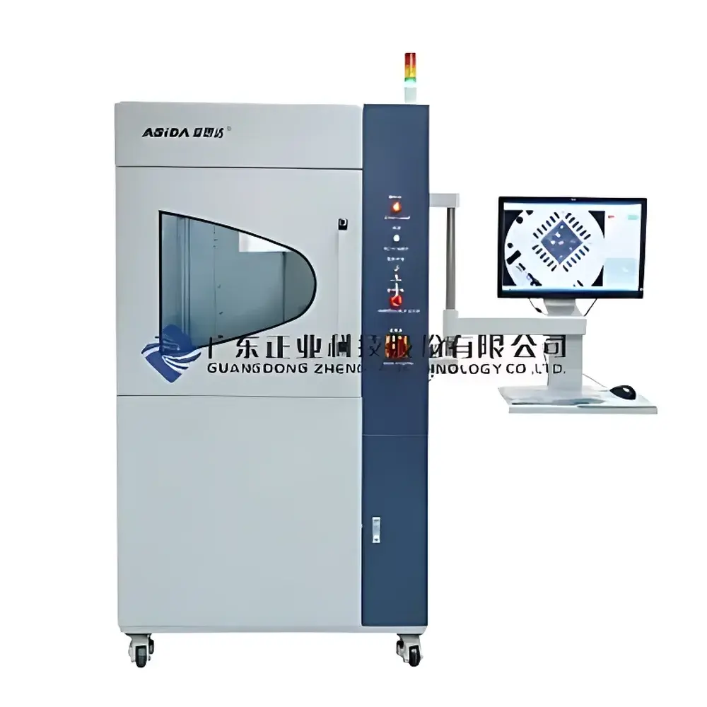
| System Dimensions | 1028 × 1025 × 1840 mm |
| Weight | ~760 kg |
| Power Supply | AC 250 V, 10 A |
| Operating Temperature | 22 ± 3 °C |
| Compliance | CE, RoHS, GB/T 18871-2002 (China National Radiation Safety Standard) |
Overview
The Zhengye XG5000 is a high-precision industrial micro-computed tomography (micro-CT) system engineered for non-destructive internal inspection and dimensional metrology of small-to-medium-sized components. It employs a sealed, integrated 90 kV microfocus X-ray tube operating under controlled vacuum conditions, enabling high-contrast radiographic imaging via absorption-based contrast mechanisms. The system leverages geometric magnification—achieved by precise manipulation of source-to-object and object-to-detector distances—to resolve sub-100 µm structural features without physical sectioning. Designed for laboratory and production-floor deployment, the XG5000 supports quantitative failure analysis (FA), void detection, solder joint integrity verification, and internal geometry validation across electronics, battery cells, precision castings, and hermetically sealed assemblies. Its architecture complies with international radiation safety benchmarks (IEC 61331-1, ISO 4037, and GB/T 18871-2002), ensuring operator protection during routine operation.
Key Features
- Sealed microfocus X-ray tube with integrated high-voltage power supply—eliminates periodic maintenance, ensures long-term beam stability, and minimizes thermal drift.
- Precision motion control system utilizing ground ball screws and synchronous stepper-driven axes (X/Y/Z), delivering repeatable positioning accuracy within ±5 µm over full travel range.
- Automatic X-ray tube shutdown after 20 minutes of inactivity, coupled with real-time tube-on-time logging for predictive maintenance scheduling.
- Interlocked safety cabinet: All access doors feature dual-channel electromagnetic interlocks that immediately terminate X-ray emission and disable high voltage upon door opening—fully compliant with EN 61000-6-4 and IEC 62471.
- Intuitive software interface with dynamic image navigation: mouse-click recentering, scroll-wheel zoom, on-screen calibration rulers, and color-coded X-ray enable/disable toggle.
- Optional tilt-axis rotation and auto-navigation path programming for multi-angle projection acquisition—facilitating 3D reconstruction workflows.
Sample Compatibility & Compliance
The XG5000 accommodates samples up to Ø150 mm × H100 mm (standard configuration), including PCBAs with BGA/CSP/flip-chip packages, lithium-ion pouch and cylindrical cells, aluminum die-cast housings, ceramic capacitors, and metal heat pipes. Its radiation shielding enclosure meets Class II medical device housing requirements per IEC 61331-1, with verified leakage ≤1 µSv/hr at 5 cm from any surface. System documentation supports GLP/GMP-aligned audit trails—including user login logs, exposure parameter records, and image metadata timestamps—enabling traceability for regulated industries such as automotive electronics (IATF 16949), medical device manufacturing (ISO 13485), and battery QA per UL 1642 and UN 38.3 test protocols.
Software & Data Management
The proprietary acquisition and analysis suite runs natively on Windows OS (Windows 10 LTSB recommended; backward-compatible with Windows 7/8.1) and supports DICOM export, TIFF/RAW pixel data dumps, and CSV-formatted measurement reports. All image annotations—including calibrated distance, area, and void volume quantifications—are embedded in EXIF metadata. Software enforces role-based access control (RBAC), session logging, and electronic signature support aligned with FDA 21 CFR Part 11 requirements when deployed with validated IT infrastructure. Raw projection datasets can be exported for third-party reconstruction (e.g., Dragonfly, Avizo, or custom MATLAB pipelines), preserving full bit-depth fidelity (16-bit grayscale).
Applications
- Semiconductor packaging: Detection of wire bond lift-off, mold compound delamination, and interlayer voids in QFN, WLCSP, and SiP modules.
- PCBA quality assurance: Identification of solder bridging, head-in-pillow defects, tombstoning, and insufficient fill in through-hole and SMT joints.
- Battery R&D: Quantification of electrode coating thickness uniformity, separator wrinkling, anode/cathode particle cracking, and electrolyte distribution in dry-room-assembled cells.
- Automotive electronics: Structural verification of sensor housings, connector crimp integrity, and thermal interface material (TIM) coverage in ADAS modules.
- Metal casting inspection: Porosity mapping, inclusion localization, and wall thickness deviation analysis in aluminum and magnesium alloy components (ASTM E155, ISO 10675-2).
- LED and optoelectronic packaging: Lens alignment verification, phosphor layer homogeneity assessment, and bond wire deformation detection.
FAQ
Is the XG5000 certified for use in ISO 17025-accredited laboratories?
Yes—the system’s mechanical repeatability, radiation output stability, and software audit-trail functionality have been validated against ISO/IEC 17025:2017 Clause 6.4 (Equipment) and Clause 7.7 (Reporting of Results) when operated under documented SOPs.
Can the system perform quantitative density analysis?
While the XG5000 delivers high-fidelity attenuation contrast, absolute density calibration requires reference phantoms and beam-hardening correction algorithms not included in standard firmware; however, relative density gradients and void fraction calculations are fully supported.
What is the typical throughput for a full 360° CT scan of a smartphone PCB?
At 1200 projections, 1024 × 1024 resolution, and 300 ms exposure per frame, acquisition time is approximately 6–8 minutes; reconstruction time varies between 4–12 minutes depending on voxel size and GPU acceleration configuration.
Does the system support automated defect classification using AI models?
The base software does not include embedded machine learning inference; however, raw projection and reconstructed volume data are accessible via API for integration with external TensorFlow/PyTorch pipelines trained on customer-specific defect libraries.
Is remote diagnostics and firmware update capability available?
Yes—secure SSH-enabled remote access (with customer-configurable firewall rules) allows authorized service engineers to monitor subsystem health, retrieve error logs, and deploy firmware patches without onsite intervention.


