
Zhengye XG5010 ASIDA High-Resolution Non-Destructive X-ray Inspection System for IC and Semiconductor Packaging Analysis
| Brand | Zhengye |
|---|---|
| Origin | Guangdong, China |
| Manufacturer Type | OEM/ODM Manufacturer |
| Country of Origin | China |
| Model | XG5010 |
| Pricing | Upon Request |
Overview
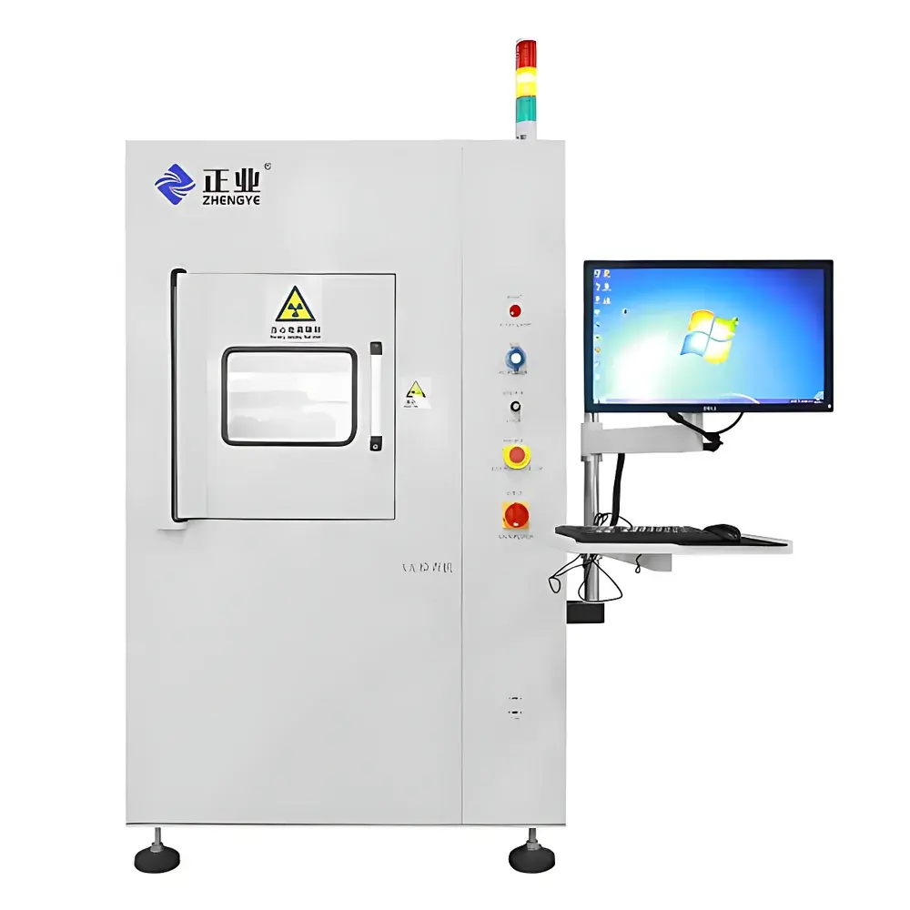
The Zhengye XG5010 ASIDA is a high-resolution, non-destructive X-ray inspection system engineered specifically for failure analysis, quality assurance, and process validation in microelectronic packaging. It operates on the principle of differential X-ray absorption—where photons generated by a sealed microfocus X-ray tube (typically operating at adjustable kV and µA settings) penetrate sample materials at varying attenuation rates, enabling real-time radiographic imaging of internal structures without physical disassembly. Unlike macro-scale industrial CT systems, the XG5010 employs a fixed geometry with high-magnification optical coupling between the scintillator screen and digital CMOS detector, delivering sub-micron feature resolution suitable for detecting wire bond misalignment, die attach voids, solder ball integrity in BGA packages, and die orientation anomalies. Its design conforms to the functional requirements of IPC-A-610, J-STD-001, and JEDEC standards for electronic assembly inspection, supporting both R&D labs and high-volume production QA environments.
Key Features
- Sealed microfocus X-ray source with stable focal spot size (<5 µm), optimized for high-contrast imaging of fine-pitch interconnects and thin-die structures
- High-luminance cesium iodide (CsI) scintillator coupled to a low-noise 5-megapixel CMOS detector for enhanced signal-to-noise ratio and dynamic range
- Motorized XYZ translation stage with ±0.1 µm repeatability and programmable tilt/rotation for multi-angle oblique viewing (0°–75°)
- Real-time digital image acquisition at up to 30 fps, with hardware-based contrast enhancement and edge sharpening algorithms
- Integrated radiation shielding compliant with GBZ 117–2020 (Chinese national standard for X-ray equipment safety) and IEC 61000-6-3 EMC emission limits
- Modular mechanical architecture supporting optional add-ons including automated defect recognition (ADR) modules and GLP-compliant audit trail logging
Sample Compatibility & Compliance
The XG5010 accommodates substrates ranging from bare silicon dies (≤20 mm × 20 mm) to full PCBAs (up to 300 mm × 300 mm), including QFN, SOIC, CSP, WLP, and stacked-die packages. It supports inspection of lithium-ion battery electrodes, ceramic capacitors, and MEMS devices—enabling cross-industry use in semiconductor fabs, contract manufacturers, and battery cell qualification labs. All operational protocols adhere to ISO/IEC 17025 general requirements for testing laboratories, with documented traceability to NIST-traceable X-ray dosimetry references. The system includes configurable exposure time, kV, and current parameters to meet material-specific penetration depth requirements while minimizing beam-induced damage to sensitive organic layers or underfill compounds.
Software & Data Management
ASIDA VisionPro™ software provides calibrated measurement tools—including line profile analysis, void area quantification, bond wire length/diameter estimation, and BGA solder joint ellipticity assessment—with uncertainty reporting per GUM (Guide to the Expression of Uncertainty in Measurement). Image metadata (kV, µA, exposure time, stage coordinates, timestamp) is embedded in DICOM-compatible files. For regulated environments, optional 21 CFR Part 11 compliance packages include role-based user authentication, electronic signatures, and immutable audit trails for all image acquisition, annotation, and report generation events. Raw data export supports TIFF, PNG, and HDF5 formats; batch processing workflows integrate with MES via RESTful API.
Applications
- Non-destructive verification of die attach integrity and void content in power modules (per AEC-Q102)
- Wire bond loop height, sweep, and tail lift evaluation in automotive ICs
- BGA and LGA solder joint bridging, head-in-pillow (HIP), and tombstoning detection
- Post-reflow and post-thermal cycling structural degradation assessment
- Failure root cause analysis (RCA) for field return units without decapsulation
- Qualification of advanced packaging technologies: Fan-Out Wafer-Level Packaging (FOWLP), 2.5D/3D IC stacking, and TSV alignment verification
FAQ
What is the minimum detectable void size in epoxy mold compound (EMC)?
Typical detection limit is ~25 µm diameter under optimal magnification and contrast settings, depending on EMC density and X-ray energy.
Does the system support automated pass/fail classification?
Yes—optional AI-assisted defect classification module enables rule-based or supervised learning models trained on customer-specific defect libraries.
Is remote operation and diagnostics supported?
Standard Ethernet interface enables secure remote desktop access and firmware update capability via TLS-encrypted connection.
Can the XG5010 be integrated into an SPC workflow?
Yes—statistical process control data (e.g., void area %, bond wire length variance) can be exported hourly to external databases or dashboards via ODBC or CSV.
What regulatory documentation is provided with shipment?
Each unit ships with Factory Acceptance Test (FAT) report, radiation safety certification, CE Declaration of Conformity (for EU export variants), and ISO 9001-certified manufacturing records.