ZOLIX SPM300 Series Semiconductor Parameter Analyzer
| Brand | ZOLIX |
|---|---|
| Model | SPM300 |
| Measurement Principle | Confocal Raman Spectroscopy |
| Spatial Resolution | < 800 nm (typical) |
| Laser Source | Standard 532 nm, 100 mW |
| Spectrometer | 320 mm focal length, imaging-corrected, spectral range 90–9000 cm⁻¹, resolution 2 cm⁻¹ |
| Sample Stage | Motorized XYZ stage, 75 × 50 mm travel, 1 µm positioning accuracy |
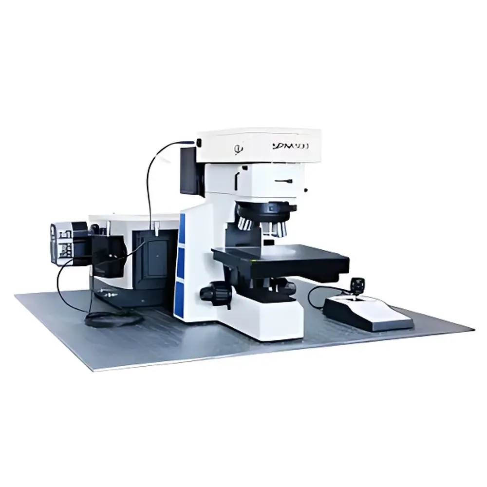
| Microscope | Upright research-grade metallurgical microscope with epi-illuminated brightfield/darkfield, standard 10×/50×/100× objectives |
| Detector | Back-illuminated deep-depletion CCD, 200–1100 nm, peak QE > 90% |
| Software | Integrated Raman data acquisition, multi-peak fitting, carrier concentration (10¹⁷–10²⁰ cm⁻³), stress mapping (±0.002 cm⁻¹), crystallinity quantification, and spatial uniformity analysis |
Overview
The ZOLIX SPM300 Series Semiconductor Parameter Analyzer is a confocal micro-Raman spectroscopy platform engineered for quantitative, non-contact, and non-destructive characterization of semiconductor materials at the microscale. It operates on the fundamental principle of inelastic light scattering—where incident monochromatic laser photons interact with lattice vibrations (phonons) in crystalline or polycrystalline semiconductors, generating Raman-shifted signals that encode information about crystal structure, strain state, doping concentration, and phase composition. Unlike conventional electrical probing methods, this optical approach eliminates sample preparation artifacts, contact resistance errors, and probe-induced damage—making it ideal for process development, failure analysis, and inline quality assurance in both R&D laboratories and high-mix semiconductor fabrication environments.
Key Features
- Confocal optical architecture with <800 nm lateral spatial resolution (typical), enabling micro-area analysis of device features such as gate stacks, epitaxial layers, and heterojunction interfaces.
- Modular laser interface box supporting up to four motorized laser channels (e.g., 488 nm, 532 nm, 633 nm, 785 nm), each with independent power control and automated wavelength switching—ensuring optimal excitation for diverse material systems (Si, SiC, GaN, Ge, MoS₂, perovskites).
- Upright metallurgical microscope with epi-illuminated brightfield/darkfield capability and standard 10×, 50×, and 100× objective lenses; optional open-frame configuration for integration with cryostats, AFM, or probe stations.
- High-throughput optical coupling: Standard CCD–slit imaging mode ensures maximum light collection efficiency; optional fiber-based confocal coupling available for enhanced axial resolution and depth sectioning.
- Precision motorized XYZ stage (75 × 50 mm travel, 1 µm repeatability) with programmable raster scanning—enabling automated mapping of carrier concentration, stress distribution, and crystallinity across wafers up to 300 × 300 mm (with extended stage option).
- Back-illuminated deep-depletion CCD detector (200–1100 nm), delivering >90% quantum efficiency at key Raman bands and low read noise—critical for weak signal detection in low-doped or thin-film samples.
Sample Compatibility & Compliance
The SPM300 supports a broad range of semiconductor substrates and devices—including silicon wafers (bulk, SOI, strained-Si), compound semiconductors (GaN-on-sapphire, SiC, InP), 2D materials (graphene, TMDs), and emerging photovoltaic absorbers (CIGS, perovskites). Its non-invasive nature complies with ISO/IEC 17025 requirements for calibration traceability in accredited labs and aligns with ASTM E1840 and ISO 21348 standards for Raman spectral measurement protocols. For regulated environments, the system’s software audit trail, user access controls, and electronic signature support are configurable to meet FDA 21 CFR Part 11 and GLP/GMP documentation requirements.
Software & Data Management
The proprietary ZOLIX RamanSuite™ software provides end-to-end workflow automation—from hardware synchronization and spectral acquisition to multivariate curve fitting and quantitative parameter extraction. Built-in algorithms perform automated peak identification, Lorentzian/Gaussian deconvolution, and physics-based modeling (e.g., phonon frequency vs. stress calibration curves, Fano line shape analysis for carrier density). Results—including carrier concentration maps (10¹⁷–10²⁰ cm⁻³), stress magnitude/direction (±0.002 cm⁻¹ precision), crystallinity index, and grain size estimation—are exported in standardized formats (CSV, HDF5, TIFF) compatible with LIMS and MES platforms. All processing steps are logged with timestamps, operator ID, and instrument configuration metadata to ensure full data provenance.
Applications
- Strain engineering validation in advanced CMOS and FinFET structures via Si–Si optical phonon shift mapping.
- Doping uniformity assessment across 200 mm and 300 mm Si wafers using carrier-induced Raman linewidth broadening analysis.
- Crystallinity grading of poly-Si thin films in TFT backplanes and solar cell absorbers through multi-peak fitting of transverse optical (TO) and longitudinal optical (LO) modes.
- Interface stress profiling at heteroepitaxial junctions (e.g., AlGaN/GaN HEMT buffers) using polarization-resolved Raman spectroscopy.
- In-line monitoring of annealing processes by tracking time-resolved evolution of Raman peak positions and intensities during thermal treatment.
FAQ
What laser wavelengths are supported, and how many can be used simultaneously?
The system supports up to four laser sources (e.g., 488 nm, 532 nm, 633 nm, 785 nm) with motorized selection—only one laser is active at a time to avoid spectral crosstalk and detector saturation.
Can the SPM300 quantify carrier concentration in heavily doped Si without reference standards?
Yes—the software implements first-principles modeling of asymmetric Raman line broadening and Fano resonance effects, enabling absolute carrier density quantification from single-spectrum analysis without empirical calibration curves.
Is the system compatible with vacuum or low-temperature stages?
Yes—both the SPM300-OM532 open-frame configuration and custom optical port layouts facilitate integration with cryogenic probe stations (4 K–300 K) and environmental chambers (vacuum, N₂, forming gas).
How is spectral calibration maintained over long-term operation?
The spectrometer includes an internal neon-argon reference lamp and automated wavelength calibration routine, traceable to NIST SRM 2035, with recalibration triggered by temperature drift thresholds or user-defined schedule.
Does the system support batch processing of multiple wafers with minimal operator intervention?
Yes—via scriptable acquisition sequences, coordinate-based wafer alignment (using integrated brightfield imaging), and auto-focus routines, unattended mapping of up to 25 wafers per run is achievable with full metadata logging.


