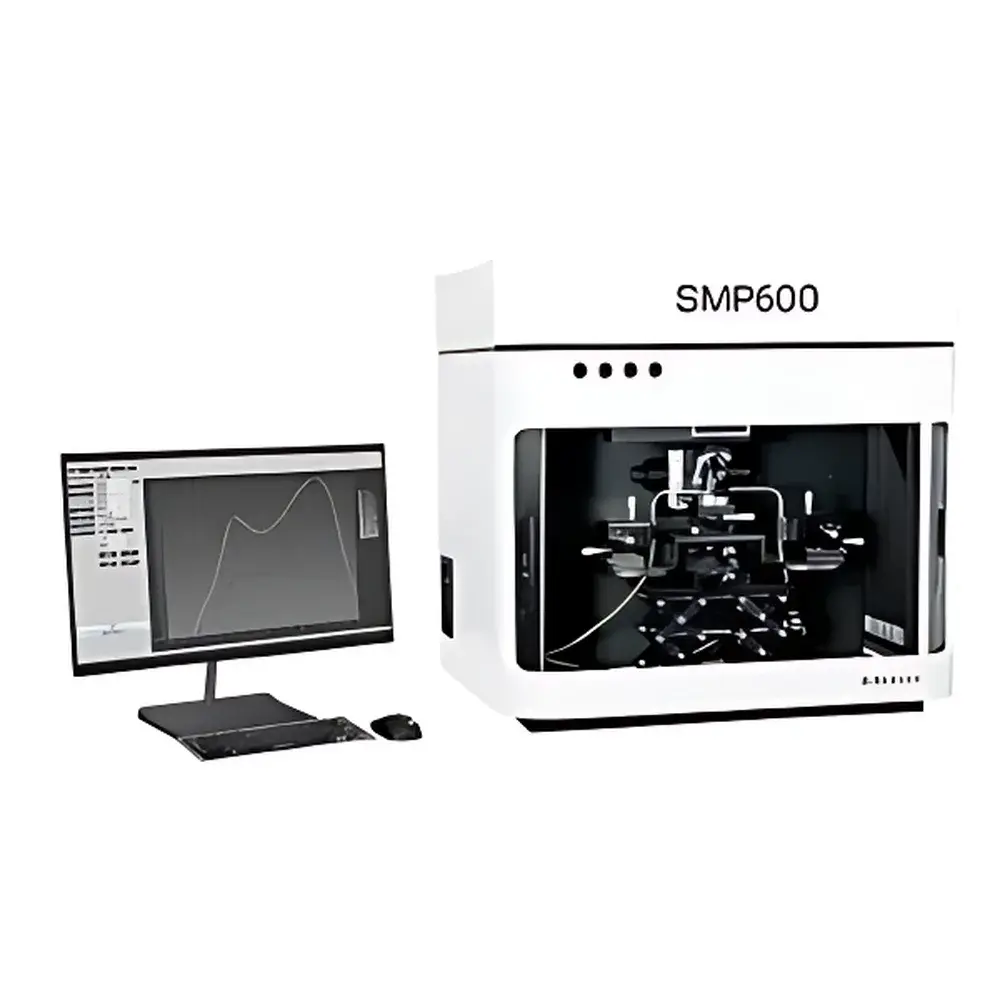
ZOLIX SPM600 Series Semiconductor Parameter Analyzer
| Brand | ZOLIX |
|---|---|
| Model | SPM600 |
| Origin | Beijing, China |
| Instrument Type | Semiconductor Photoelectrical Characterization System |
| Light Source Options | EQ Lamp (190–1700 nm), Xenon Lamp (250–1700 nm), Xenon–Halogen Composite Lamp (250–2500 nm) |
| Spectral Resolution | Adjustable via monochromator (typical <1 nm FWHM) |
| Spot Size | 40 µm (diffraction-limited at visible/NIR) |
| Temporal Resolution | Down to 200 ms for irradiance-dependent I–t sweeps |
| Compliance | Designed for ISO/IEC 17025-aligned lab environments |
Overview
The ZOLIX SPM600 Series Semiconductor Parameter Analyzer is a benchtop photoelectrical characterization platform engineered for quantitative, traceable measurement of optoelectronic properties in semiconductor materials and micro/nanoscale devices. It operates on the principle of monochromated spectral excitation coupled with synchronized high-fidelity current–voltage (I–V), current–time (I–t), and voltage–time (V–t) acquisition under controlled bias and irradiance conditions. Unlike generic optical power meters or standalone source-measure units, the SPM600 integrates calibrated spectral irradiance delivery, sub-millisecond temporal sampling, and spatially resolved scanning—enabling absolute spectral responsivity (A/W), external quantum efficiency (EQE), carrier lifetime, diffusion length, and mobility extraction without reliance on reference detectors. Its architecture adheres to metrological best practices for photodetector calibration, supporting both research-grade device physics investigations and pre-compliance screening for photodiode, perovskite solar cell, and 2D material phototransistor development.
Key Features
- Monochromator-coupled broadband excitation (190–2500 nm) with selectable light sources: EQ lamp (UV-enhanced, 190–1700 nm), xenon arc lamp (high-intensity, 250–1700 nm), or xenon–halogen composite (extended NIR, 250–2500 nm)
- Diffraction-limited 40 µm spot size optimized for pixel-level characterization of micro-patterned photodetectors and focal-plane arrays
- Simultaneous multi-parameter acquisition: spectral responsivity (A/W), monochromatic I–V, irradiance-dependent I–t (200 ms resolution), bias-dependent transient response, and LBIC mapping
- Programmable DC/AC biasing up to ±30 V with sub-mV resolution, enabling dark current analysis, junction barrier assessment, and trap-state probing
- Modular optical path design accommodating optional accessories: beam splitters for pump–probe configurations, fiber-coupled inputs for laser integration, and environmental chamber interfaces
- Thermally stabilized optical bench and low-drift current preamplifiers (<10 fA noise floor) ensure measurement repeatability over extended acquisition windows (≥8 h continuous operation)
Sample Compatibility & Compliance
The SPM600 accommodates planar semiconductor devices ranging from discrete photodiodes and thin-film phototransistors to wafer-level test structures and packaged optoelectronic modules. Sample mounting uses vacuum chuck or kinematic stage options compatible with standard probe stations (e.g., Cascade Microtech, MPI). All optical calibrations are traceable to NIST-traceable reference photodiodes (e.g., Hamamatsu S1337 series) and spectral irradiance standards. The system supports documentation workflows aligned with ISO/IEC 17025 requirements, including instrument calibration certificates, uncertainty budgets for responsivity measurements (k=2), and audit-ready metadata logging. While not FDA-certified as a medical device, its data integrity framework—including user access control, electronic signatures, and immutable audit trails—meets foundational expectations for 21 CFR Part 11 readiness in regulated R&D settings.
Software & Data Management
Control and analysis are performed via ZOLIX’s proprietary SPMControl Suite (Windows-based, 64-bit), which implements a modular, scriptable acquisition engine compliant with IEEE 1278.1 (HDF5-based data serialization). Each measurement session auto-generates timestamped HDF5 files containing raw waveforms, metadata (wavelength, bias, irradiance, ambient temperature), and processing history. Batch analysis tools enable automated EQE calculation per ASTM E1021, spectral responsivity interpolation per CIE S 026/E:2018, and transient decay fitting using multi-exponential models (τ₁, τ₂, amplitude ratios). Export formats include CSV, MATLAB .mat, and industry-standard JDX for spectral databases. Optional Python API enables integration into CI/CD pipelines for automated qualification testing.
Applications
- Quantitative spectral responsivity mapping of CMOS image sensor pixels and InGaAs focal plane arrays
- Carrier transport parameter extraction: diffusion length (from transient photocurrent rise/fall kinetics), mobility (via time-of-flight analysis under pulsed excitation), and recombination lifetime (from open-circuit voltage decay)
- Linearity validation of photodetectors across 6+ decades of irradiance (10⁻⁸–10² W/m²), critical for radiometric calibration labs
- LBIC (Light Beam Induced Current) imaging of grain boundaries and defect clusters in polycrystalline perovskites and CIGS absorbers
- Stability assessment of emerging optoelectronics under ISOS-L-1 illumination protocols, with real-time degradation trending
- Pre-screening of novel photovoltaic absorbers (e.g., organic–inorganic hybrids, quantum dot films) prior to full-cell fabrication
FAQ
Does the SPM600 support pulsed laser excitation?
Yes—via optional fiber-coupled input port and external trigger synchronization (TTL-compatible), enabling integration with picosecond lasers for time-resolved photocarrier dynamics studies.
Can spectral responsivity be measured traceably without a NIST-calibrated reference detector?
No—the system requires periodic calibration against a NIST-traceable photodiode; built-in routines guide users through irradiance calibration using certified reference standards.
Is the 40 µm spot size adjustable?
The minimum spot is fixed at 40 µm (limited by diffraction and monochromator exit slit); optional beam expanders or focusing optics can increase spot size up to 500 µm for macroscopic sample averaging.
What level of uncertainty is achievable in EQE measurement?
Typical expanded uncertainty (k=2) is ±2.3% for silicon-based detectors at 633 nm, based on combined contributions from spectral irradiance calibration, current measurement accuracy, and geometric factor determination.
Does the software comply with 21 CFR Part 11 for electronic records?
The core acquisition software provides audit trail generation and user authentication; full Part 11 compliance requires site-specific validation protocol execution and IT infrastructure alignment (e.g., secure network storage, backup policies).


