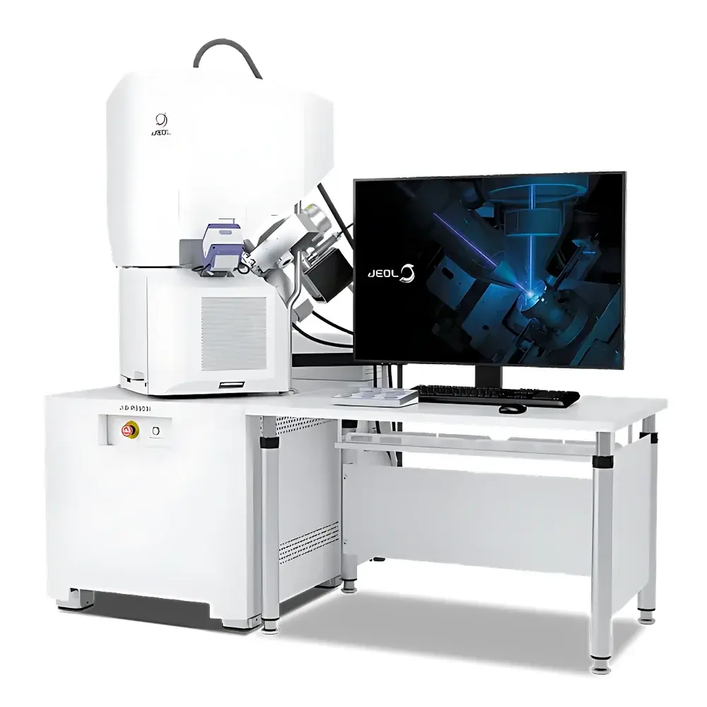
JEOL JIB-PS500i High-Precision Focused Ion Beam (FIB) System
| Brand | JEOL |
|---|---|
| Origin | Japan |
| Model | JIB-PS500i |
| Electron Beam Resolution | 0.7 nm @ 15 kV, 1.0 nm @ 1 kV |
| Ion Beam Resolution | 3 nm |
| Maximum Ion Beam Current | 100 nA |
| Maximum Electron Beam Current | 500 nA |
Overview
The JEOL JIB-PS500i is a high-precision dual-beam focused ion beam (FIB) system engineered for nanoscale sample preparation, cross-sectional imaging, circuit edit, and in situ analytical workflows. Combining a field-emission scanning electron microscope (FE-SEM) with a liquid metal ion source (LMIS) gallium ion column, the JIB-PS500i operates on the principle of sequential or simultaneous electron imaging and ion milling—enabling real-time observation of material modification at sub-nanometer scale. Its architecture supports seamless integration with transmission electron microscopes (TEM), allowing for lift-out, thinning, and transfer of electron-transparent lamellae directly into TEM holders—a critical capability for advanced materials science, semiconductor failure analysis, and life sciences correlative microscopy.
Key Features
- Sub-nanometer electron beam resolution: 0.7 nm at 15 kV and 1.0 nm at 1 kV, optimized for high-fidelity surface topography and low-voltage imaging of beam-sensitive specimens.
- High-current dual-beam capability: Electron beam current up to 500 nA enables rapid imaging, EDS mapping, and electron-induced deposition; ion beam current up to 100 nA supports aggressive milling, trenching, and bulk removal without compromising positional accuracy.
- Ion beam resolution of 3 nm ensures precise feature definition during nanostructuring, maskless lithography, and site-specific ablation—critical for device-level metrology and quantum device fabrication.
- Fully automated software suite includes intelligent stage navigation, pattern-based milling recipes, auto-alignment routines for electron/ion beam co-registration, and real-time dose monitoring to minimize redeposition and curtailing artifacts.
- Dedicated TEM interface module facilitates standardized mechanical and electrical coupling with JEOL and third-party TEM systems, including vacuum interlock synchronization, coordinate mapping, and automated lamella transfer protocols compliant with standard TEM grid geometries.
Sample Compatibility & Compliance
The JIB-PS500i accommodates a broad range of solid-state samples—including Si wafers, compound semiconductors (GaN, SiC), battery cathode/anode composites, geological thin sections, and cryo-fixed biological tissues—within a maximum specimen size of Ø150 mm × 50 mm height. Stage motion supports ±60° tilt, 360° rotation, and 5-axis motorized precision control (sub-10 nm repeatability). The system complies with IEC 61000-6-3 (EMC emission standards) and ISO 14644-1 Class 5 cleanroom operational guidelines. Vacuum architecture maintains base pressure <5×10⁻⁸ Pa in the ion column and <2×10⁻⁶ Pa in the main chamber, ensuring minimal contamination during extended FIB-SEM sessions. All automation scripts and parameter logs are timestamped and exportable to support GLP/GMP documentation requirements.
Software & Data Management
Control and data acquisition are managed via JEOL’s proprietary JIB-PS software platform, built on a modular, client-server architecture supporting remote operation and multi-user session management. The software provides full audit trail functionality—including user login history, parameter change logs, and recipe execution timestamps—aligned with FDA 21 CFR Part 11 electronic record integrity requirements. Image and spectral datasets (EDS, EBSD, CL) are stored in vendor-neutral formats (TIFF, HDF5, MRC) and can be exported directly to third-party analysis tools such as DigitalMicrograph, HyperSpy, or MATLAB. Real-time image stitching, drift correction, and machine-learning-assisted feature recognition (e.g., grain boundary detection, pore segmentation) are available as optional licensed modules.
Applications
- Semiconductor process development: Cross-sectioning of FinFETs, nanowires, and 3D NAND stacks for defect localization and metrology.
- Advanced battery research: In situ ion milling of cycled electrode particles to expose SEI/CEI interfaces for compositional and structural analysis.
- Materials science: Site-specific TEM lamella preparation from polycrystalline alloys, MAX phases, and irradiated nuclear fuels.
- Geosciences: Nanoscale textural analysis of meteoritic chondrules and metamorphic mineral assemblages under ultra-high vacuum conditions.
- Life sciences: Cryo-FIB milling of vitrified cells followed by CLEM (correlative light-electron microscopy) registration using fiducial markers.
FAQ
Is the JIB-PS500i compatible with non-JEOL TEM systems?
Yes—the system employs standardized flange interfaces (CF100/CF150) and supports custom vacuum interlock signaling protocols for integration with Thermo Fisher, Hitachi, and Zeiss TEM platforms.
Does the software support automated lamella thickness control?
Yes—real-time secondary electron yield monitoring combined with ion dose feedback enables closed-loop thickness regulation down to ±2 nm tolerance.
Can the system perform gas-assisted etching or deposition?
The JIB-PS500i supports optional integrated gas injection systems (GIS) for Pt/C/W deposition and XeF₂-enhanced Si etching, configurable via software-controlled valve sequencing.
What is the typical service interval for the Ga⁺ ion source?
Under standard operating conditions (≤50 nA average current, 8 h/day usage), the LMIS source achieves ≥12 months of stable emission before recalibration or replacement.
Is remote diagnostics supported?
Yes—JEOL’s SecureLink™ remote maintenance protocol allows authorized engineers to perform firmware updates, calibration checks, and fault diagnostics over encrypted TLS 1.3 connections.


