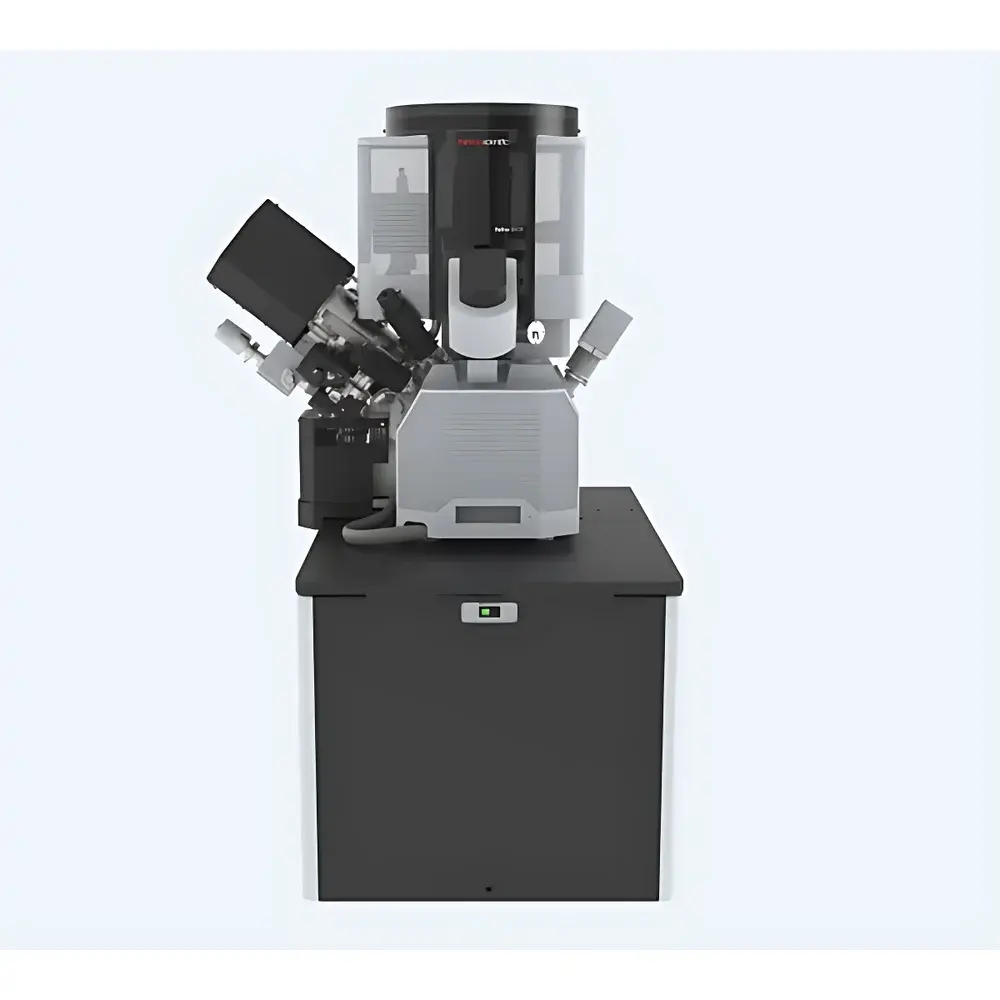
Thermo Fisher Scientific Helios NanoLab DualBeam™ Scanning Electron Microscope
| Brand | Thermo Fisher Scientific |
|---|---|
| Origin | Czech Republic |
| Manufacturer Type | Original Equipment Manufacturer (OEM) |
| Origin Category | Imported |
| Model | Helios NanoLab DualBeam™ |
| Price Range | USD 1.3M – 1.9M |
Overview
The Thermo Fisher Scientific Helios NanoLab DualBeam™ is a high-performance, integrated scanning electron microscope (SEM) and focused ion beam (FIB) platform engineered for nanoscale characterization, precision sample preparation, and in situ nanofabrication. Leveraging advanced electron optics and gallium liquid-metal ion source (LMIS) FIB technology, the system enables simultaneous or sequential imaging, milling, deposition, and analysis at sub-nanometer resolution. Its dual-beam architecture supports correlative workflows across materials science, semiconductor metrology, geoscience, and structural biology—where spatial registration between SEM imaging and FIB sectioning is critical for accurate 3D reconstruction, TEM lamella preparation, and site-specific prototyping.
Key Features
- Sub-nanometer SEM resolution with through-the-lens (TTL) and in-column secondary electron (SE) detectors for high-contrast, low-voltage surface imaging
- High-brightness Schottky field-emission electron source optimized for stability and signal-to-noise ratio at accelerating voltages from 0.1 kV to 30 kV
- Ultra-stable gallium FIB column with beam current range from 1 pA to 65 nA, enabling both high-resolution imaging and high-throughput milling
- Precision piezo-driven stage with <1 nm positional repeatability and active drift compensation for long-duration serial sectioning
- Integrated gas injection systems (GIS) for electron- and ion-beam-induced deposition (EBID/IBID) of Pt, C, and W, supporting circuit edit, lift-out, and protective cap formation
- Dual-chamber configurations available: standard chamber (for general-purpose research) and large-chamber variant (optimized for oversized wafers, geological cores, or multi-sample holders)
Sample Compatibility & Compliance
The Helios NanoLab accommodates diverse specimen geometries—from 3 mm TEM grids and 300 mm silicon wafers to irregular rock fragments and frozen-hydrated biological tissues (when used with cryo-transfer accessories). All hardware and software modules comply with ISO 14644-1 Class 5 cleanroom requirements for semiconductor applications. The system supports audit-ready operation under GLP and GMP frameworks, with optional 21 CFR Part 11-compliant software packages that enforce electronic signatures, user access control, and immutable audit trails for image acquisition, milling scripts, and metadata logging. It meets ASTM E1558 (standard guide for FIB sample preparation) and ISO/IEC 17025 traceability requirements when calibrated using NIST-traceable reference standards.
Software & Data Management
Control and analysis are unified via Thermo Fisher’s AutoScript™ Python-based automation framework and Maps™ 4D visualization suite. AutoScript enables fully programmable, repeatable workflows—including automated lamella thinning, tilt-series acquisition, and region-of-interest (ROI) milling sequences—with error recovery and real-time feedback. Maps™ supports segmentation, quantitative porosity analysis, grain boundary mapping, and volumetric rendering of serial-section datasets (e.g., FIB-SEM tomography stacks). Raw data is stored in standardized TIFF/HDF5 formats with embedded metadata (voltage, dwell time, beam current, stage coordinates), ensuring FAIR (Findable, Accessible, Interoperable, Reusable) compliance. Integration with Thermo Fisher Connect cloud platform allows secure remote monitoring, cross-instrument data federation, and centralized license management.
Applications
- Materials Science: Multi-scale microstructural analysis of alloys, ceramics, and composites; in situ deformation studies; phase identification via integrated EDS/WDS and EBSD
- Semiconductor Industry: Failure analysis of logic and memory devices; cross-sectional imaging of FinFETs and GAA transistors; TEM sample preparation with thickness uniformity <±5 nm
- Geoscience: Pore-network quantification in shale, carbonate, and reservoir rocks; 3D mineralogical mapping via FIB-SEM tomography coupled with energy-dispersive X-ray spectroscopy (EDS)
- Life Sciences: Correlative light and electron microscopy (CLEM) workflows; serial block-face imaging of resin-embedded neural tissue; cryo-FIB milling of vitrified cells for high-resolution cellular ultrastructure
- Nanofabrication: Direct-write nanolithography; MEMS/NEMS device prototyping; maskless patterning of plasmonic metasurfaces and photonic crystals
FAQ
What vacuum levels are maintained in the electron and ion columns?
The electron column operates at ≤1×10⁻⁷ Pa, while the FIB column maintains ≤5×10⁻⁶ Pa during milling—both stabilized via differential pumping and non-evaporable getter (NEG) pumps.
Is the system compatible with third-party detectors?
Yes—via standard PCIe and Ethernet interfaces, it supports integration with external EBSD cameras, time-of-flight mass spectrometers (ToF-SIMS), and cathodoluminescence (CL) systems.
How is beam alignment and calibration performed?
Automated alignment routines are executed using built-in Faraday cup arrays and reference grids; all calibrations are traceable to NIST SRM 2090a and certified annually per ISO/IEC 17025 protocols.
Can the system perform in situ heating or electrical biasing experiments?
Yes—through optional holders including MEMS-based heating stages (up to 1200°C), nano-manipulators with four-point probe capability, and electrochemical liquid cells.
What is the typical throughput for TEM lamella preparation?
From rough milling to electron-transparent thickness (~100 nm), a single lamella can be prepared in 60–90 minutes, depending on material hardness and final thickness specification.


